A method for fabricating stacks of semiconductors just a few atoms thick offers a simple, cost-effective route to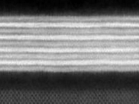 A stack of films, shown in cross-section using an electron microscope. Each is only a few atoms thick. (Courtesy of Kang et. al.) making thin, uniform layers of these materials, which could expand capabilities for electronic devices from solar cells to cell phones.
The current approach to forming these layers is to “grow” them instead of stacking one on top of one another. In this process, bottom layers have to be subjected to harsh growth conditions such as high temperatures while the new ones are added. Requirements for such conditions limit the materials which can be used.
University of Chicago and Cornell University researchers instead made the films individually by placing them in a vacuum, peeling them off, and sticking them to one another. The Post-It note assembly process enabled development of films that are connected with weak instead of stronger covalent bonds, a property which interferes less with the perfect surfaces between layers.
To test their electrical properties, the films were fashioned into devices such as band-engineered heterostructure tunnel diodes and superlattice films with vertical compositions. Analyses show that these materials can be designed and tuned on an atomic scale, which could allow them to serve as an essential component in future computer chips.
The stacked films are detachable, suspendable and compatible with water or plastic surfaces, which will enable their integration with advanced optical and mechanical systems.
