Earlier this week, IBM announced the successful development of a process to manufacture silicon nanosheet transistors that will enhance the new generation of silicon chips of five-nanometer nodes. This is an astounding result given the fact that less than two years ago they developed the 7nm node chips.
The company’s development took place at the IBM-led Research Alliance at the SUNY Polytechnic Institute Colleges of Nanoscale Science and Engineering’s NanoTech Complex in Albany, NY working with partners GLOBALFOUNDRIES and Samsung. It is expected that the chip performance and the power savings will double with this new technology. The development will be able to lead the way for 30 billion transistors in a piece of silicon the size of your fingernail, and help accelerate artificial intelligence computing, the Internet of Things (IoT), and other data-intensive cloud applications. According to the researchers, compared to the current technology (10nm) the nanosheet-based 5 nm nodes will be able to deliver four percent better performance at fixed power, or 75 percent in power savings at matched performance.
 SUNY Poly Zen building. Credit: SUNY Poly
The breakthrough was achieved by using stacks of silicon nanosheets as the main transistor structure, instead, as is the case today, of the FinFET architechture. Important for 7nm nodes.
“For business and society to meet the demands of cognitive and cloud computing in the coming years, advancement in semiconductor technology is essential,” said Arvind Krishna, senior vice president, Hybrid Cloud, and director, IBM Research. “That’s why IBM aggressively pursues new and different architectures and materials that push the limits of this industry, and brings them to market in technologies like mainframes and our cognitive systems.”
“This announcement is the latest example of the world-class research that continues to emerge from our groundbreaking public-private partnership in New York,” said Gary Patton, CTO and Head of Worldwide R&D at GLOBALFOUNDRIES. “As we make progress toward commercializing 7nm in 2018 at our Fab 8 manufacturing facility, we are actively pursuing next-generation technologies at 5nm and beyond to maintain technology leadership and enable our customers to produce a smaller, faster, and more cost efficient generation of semiconductors.”
IBM has been exploring nanosheet semiconductor technology for over 10 years without any result, until now. This is the development that shows the feasibility of stacked nanosheet devices that are more powerful than FinFET technology.
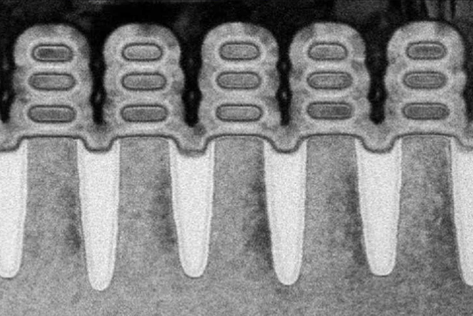 The IBM/GlobalFoundries/Samsung revolutionary 5-nanometer nano sheet transistors, with quadruple all-around-gates should give smartphones 2-to-3 day battery life. (Source: IBM)
This development is also a great achievement for SUNY Poly and the state of New York.
“Today’s announcement continues the public-private model collaboration with IBM that is energizing SUNY-Polytechnic’s, Albany’s, and New York State’s leadership and innovation in developing next generation technologies,” said Dr. Bahgat Sammakia, Interim President, SUNY Polytechnic Institute. “We believe that enabling the first 5nm transistor is a significant milestone for the entire semiconductor industry as we continue to push beyond the limitations of our current capabilities. SUNY Poly’s partnership with IBM and Empire State Development is a perfect example of how Industry, Government and Academia can successfully collaborate and have a broad and positive impact on society.”
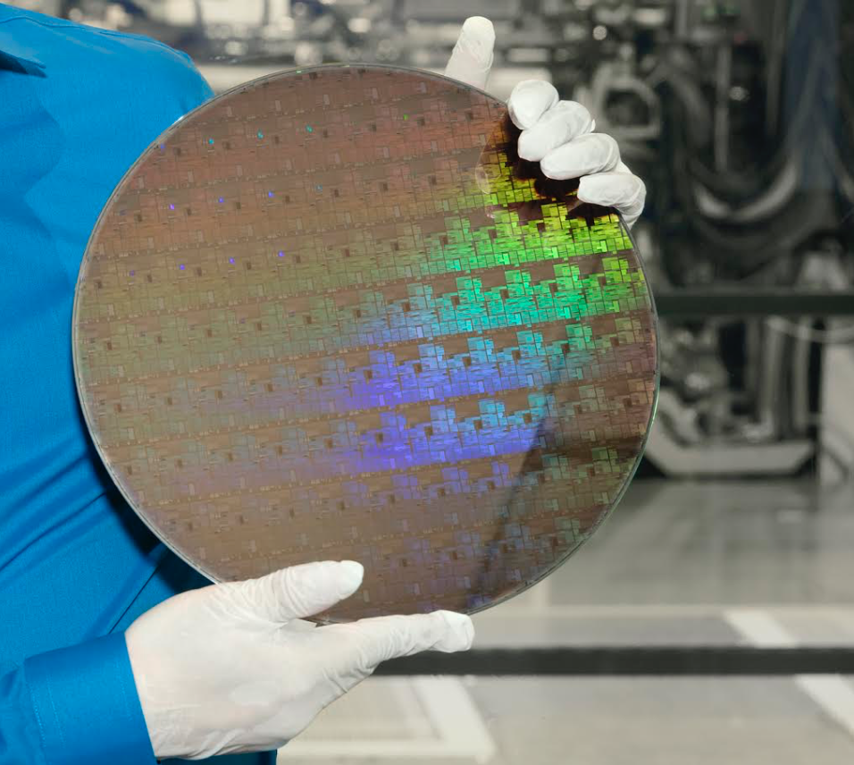 IBM Research scientist Nicolas Loubet holds a wafer of chips using 5nm silicon nanosheet transistors manufactured using an industry-first process. (Photo Credit: Connie Zhou) (Source: IBM)
The results of the research will be presented at the 2017 Symposia on VLSI Technology and Circuits conference in Kyoto, Japan (http://www.vlsisymposium.org/ ) on June 5 – 8, 2017.
