A wealth of information can reside in electronic decals—if they can be made small enough and are produced quickly, inexpensively and precisely enough. Massachusetts Institute of Technology (MIT) engineers have invented a new technique that can do exactly that. Researchers published a paper in "Science Advances" describing a stamping process that prints electronic inks onto both rigid and flexible surfaces, using a stamp made from forests of carbon nanotubes.
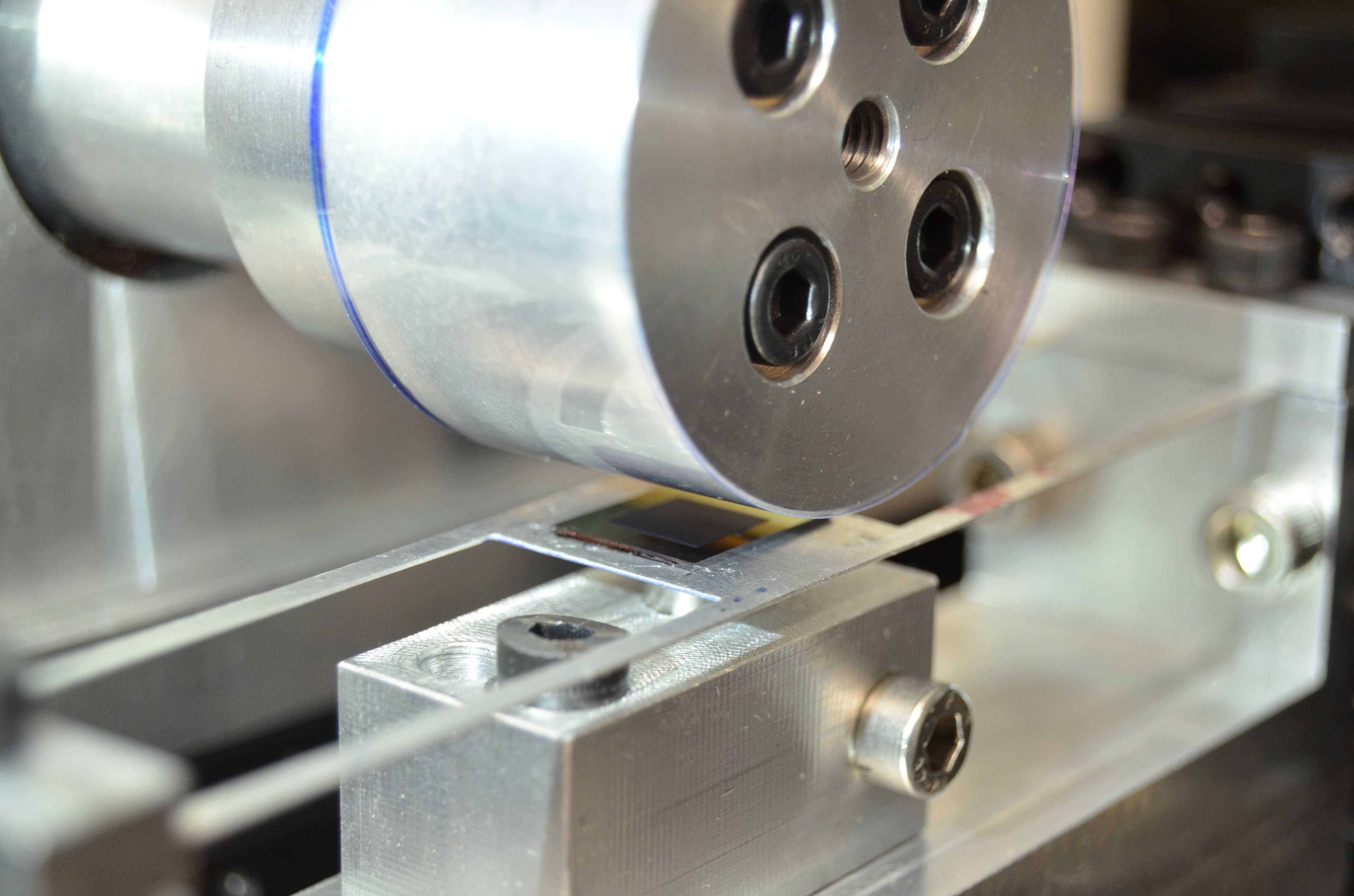 The researchers’ machine uses a nanoporous stamp through which a solution of nanoparticles can flow uniformly onto the printing surface. / Credit: Sanha Kim and Dhanushkodi Mariappan The stamping process should be able to print transistors small enough to control individual pixels in high-resolution displays and touchscreens, according to senior author A. John Hart, Mitsui Career Development Associate Professor in Contemporary Technology and Mechanical Engineering at MIT. Hart, along with lead author Sanha Kim, a postdoc in MIT’s Department of Mechanical Engineering, and their team of colleagues from MIT, helped develop the process.
“There is a huge need for printing of electronic devices that are extremely inexpensive but provide simple computations and interactive functions,” says Hart in a news release on the MIT website. “Our new printing process is an enabling technology for high-performance, fully printed electronics, including transistors, optically functional surfaces and ubiquitous sensors.”
Rubber Stamping Meets Nanotube Technology
The researchers borrowed from the established technique of rubber stamp printing, or flexography, but sought to create nanoporous stamps—spongier than conventional rubber stamps—to permit nanoparticle ink to flow through the stamp uniformly.
To make the stamps, the researchers grew carbon nanotubes in various patterns on a silicon surface, coating them with a thin polymer layer, so the ink would not penetrate and the nanotubes would retain their size after stamping. The resulting stamps were infused with electronic ink containing nanoparticles of silver, zinc oxide or semiconductor quantum dots.
The team then developed a model to predict the amount of force necessary to apply an even layer of ink onto a substrate given a number of variables, including the roughness of the stamp and substrate, and the concentration of nanoparticles in the ink.
Scaling the Technique
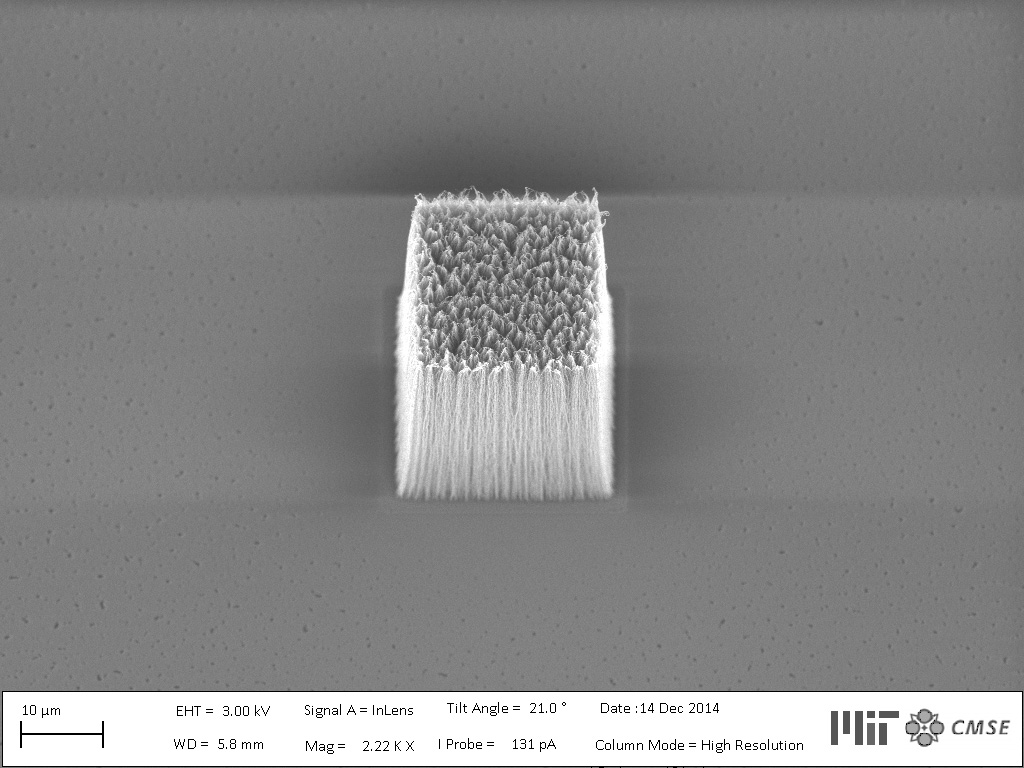 Carbon nanotubes form a highly detailed stamp to print nanoparticles onto flexible and rigid surfaces. / Credit: Sanha Kim and Dhanushkodi Mariappan The prototype, limited by the motor speed, prints at a rate of 200 millimeters per second, which Hart said is competitive with today’s industrial printing technologies.