Last week at APEC 2016 in Long Beach, CA, El Segundo, California-based startup Navitas Semiconductor unveiled its plan to deliver true gallium nitride (GaN) power ICs using its proprietary AllGaN monolithically integrated 650 V platform. Initially, employing its AllGaN process, the young company intends to combine enhancement-mode GaN power FETs with GaN logic and drive circuits on a silicon substrate. According to CEO Gene Sheridan, the company has been sampling its first GaN-on-Silicon power IC to select customers for the last few months and intends to make it commercially available in a QFN package in summer. To accomplish that, it is closely working with a large Asian foundry.
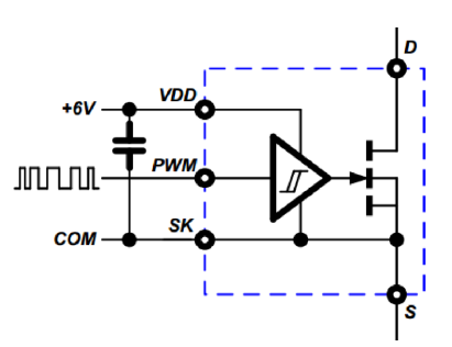 GaN-on-Si power IC combines gate drive and logic circuits with GaN power FETs on a single chip.
 Key features driving this performance include no gate loop parasitic; clean, fast gate signal; and rail-to-rail gate signal. Plus it offers high-frequency drive with minimal propagation delay. The benefits of GaN power IC are demonstrated in a 150 W boost power factor correction (PFC) circuit with universal AC input (85–265 Vac, 47–63 Hz) and 400 V, 0.27 A output. Built using two-layer PCB, it measures 100 x 50 x 20 mm and requires no heat sink. The peak measured efficiency reported by the company is 98.1% and the power factor is > 0.995 at 150 W.
Initially Navitas intends to fabricate its GaN-on-Si power ICs on a six-inch wafer with plans to migrate to eight-inch wafers in a few years. Although the company did not provide pricing for its GaN power ICs, it said the parts will be produced in low-cost standard CMOS fabs with plentiful capacity.
