Equipment maker EV Group (EVG) has introduced a 300mm wafer-bonding system for implementation into microelectromechanical systems (MEMS) high-volume manufacturing.
EVG claims its Gemini wafer-bonding system is one of the first 300mm systems used for MEMS manufacturing, as up until now the market had used smaller 200mm wafer substrates for MEMS manufacturing. The ability of the wafer bonder to support 300mm MEMS production allows for a more cost-effective implementation of emerging applications, such as CMOS-MEMS integration, EVG says.
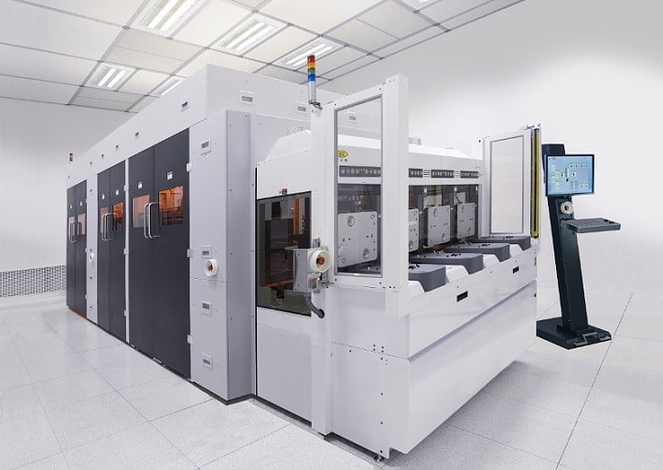 The wafer-bonding device allows for MEMS manufacturers to increase production yields as well as lower overall system costs. Source: EVGIn MEMS manufacturing, the devices have very small moving parts that must be protected from the ambient environment. High-force permanent wafer bonding allows for wafer-level capping of MEMS devices, which seals a wafer’s worth of MEMS devices in one operation, EVG says. After the devices have been capped, they can be packaged in a much simpler and lower-cost package.
Bringing this process to 300mm wafers means MEMS manufacturers can increase production yields as well as lower overall cost of production, the Austrian-based company says. Furthermore, the ability to perform permanent bonding of 300mm MEMS wafers will allow for CMOS-MEMS integration—which will allow MEMS devices to be more sophisticated—without requiring chip-to-wafer bonding or wire bonding, which can increase production costs or increase the footprint of the MEMS device, EVG says.
The Gemini 300mm wafer bonder includes EVG’s proprietary SmartView automated bond-alignment system, a modular design that allows for customization, scale and reconfiguration of systems for different bond processes, integrated wafer preparation and conditioning, including oxide removal, swap-in modules for changeover and serviceability, depending on bond-process needs, a bond-temperature threshold of up to 500 degrees Celsius, and temperature uniformity for rapid heating and cooling capability.
