
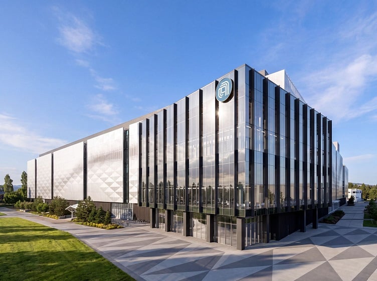
Applied Materials has unveiled the Equipment and Process Innovation and Commercialization (EPIC) Center, which the company claims is the world’s largest facility dedicated to collaborative chip process technology and manufacturing equipment R&D.
The EPIC Center will bring together chipmakers, systems vendors, equipment partners and university researchers to accelerate chip innovation for next-generation semiconductor manufacturing and equipment.
“As AI infrastructure scales, the demands of high-performance computing are driving unprecedented complexity across the chipmaking roadmap,” said Gary Dickerson, president and CEO of Applied Materials, in a statement.
“To win the race for AI leadership, our industry must rethink and re-engineer how we collaborate to develop and commercialize the next generation of semiconductor technologies.”
Applied Materials is investing $5 billion in the EPIC Center that will be a 600,000 ft2 structure that will house four acres of cleanroom space. The founding roster of the EPIC Center partners runs the gamut of technology companies and researchers including the following.
- TSMC
- Intel
- SK Hynix
- Micron
- Samsung Electronics
- Broadcom
- Advantest
- SCREEN
- KIOXIA
- Besi
- Arizona State University
- Rensselaer Polytechnic Institute
- Stanford University
- UC Berkeley
- UCLA Samueli School of Engineering
Applied Materials said it expects additional companies, organizations, universities and research hubs to join the EPIC ecosystem in the future.
“AI is creating a multi-trillion-dollar opportunity for the semiconductor industry. To capture it, we need continued innovation in transistors, interconnects and advanced packaging,” said Lip-Bu Tan, CEO at Intel. “At Intel, we see a path to more than a trillion transistors in a package by 2030. As architectures become more complex and R&D costs continue to rise, we need to move faster and work more closely with our equipment partners. EPIC gives our teams the opportunity to work side by side with Applied on materials and process innovation – helping us accelerate development, improve R&D efficiency and bring new technologies to market faster.”
