
Gallium nitride (GaN) FETs allow DC/DC converters, adapters, motor-drive stages, and high-density power modules to switch faster than comparable silicon MOSFET implementations. That speed is the reason designers are using GaN in newer applications. However, a GaN-based power stage can have high efficiency on the bench and still fail EMC, show false turn-on, or exhibit excessive ringing because the gate-drive loop, power loop, and switch-node geometry were treated like an ordinary MOSFET layout.
GaN devices have low gate-charge requirements, low gate voltage margin, and packages that are designed to expose as little parasitic inductance as possible. The lower gate margin in GaN FETs compared to Si MOSFETs creates risk of overshoot failure, and part of controlling that overshoot is reducing loop inductance in the PCB layout. The other big challenges relate to current sharing in power systems, and how the inherent properties of GaN devices impact control strategies in DC/DC converters.
Driving GaN FETs
Enhancement-mode GaN FETs are voltage-driven devices, but their gate-drive requirements are tighter than silicon MOSFETs. A typical silicon MOSFET can tolerate a relatively wide gate-voltage range, with drive voltages up to 12 V being common. Some enhancement-mode GaN devices use a gate drive voltage near 5 V, but with an absolute maximum gate rating that leaves little room for overshoot on the gate. That makes the driving GaN FET gates a switching speed problem and a voltage stability problem.
The driver has to source and sink gate current fast enough to charge and discharge the input capacitance without excessive gate ringing. Because the gate charge is low, the loop inductance and driver package inductance can create high-frequency transients. A small overshoot that would be ignored in a silicon MOSFET design can become a reliability concern in a GaN design.
From the circuit design perspective, we can see a typical gate driver connection to a GaN FET package from a datasheet example.
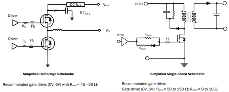 Left: half-bridge schematic example with gate drive resistor, optional ferrite bead, and high-side RC snubber. Right: single-FET (flyback) example with ON/OFF gate resistors and RCD clamp. Source: Renesas TP65H300G4LSGB datasheet
Whether the gate connection remains low-inductance depends heavily on the PCB layout. The example circuit connections shown above help potential overshoot, which is influenced by package parasitics, but the PCB layout can still introduce unwanted inductance that impacts current path connecting to the gate driver.
Additional factors that influence driving and reliability of GaN-based power electronics occur at the system level, arising with driving and monitoring the output from GaN-based power stages. This includes:
- Enforcing dead time to prevent shoot-through
- Implementing zero-voltage switching
- Preventing false turn-on from Miller coupling
- Maintaining proper gate-drive voltage margin
- Monitoring switch-node ringing and overshoot
Types of GaN FET drivers available
GaN drivers should be selected around the power-stage topology, voltage class, isolation requirement, timing control, and protection behavior. The driver category matters, but the datasheet details matter more. Peak source and sink current, common-mode transient immunity (CMTI), under-voltage lockout (UVLO) threshold, bootstrap behavior, propagation delay matching, and gate-voltage regulation all affect whether the driver can control the GaN device in the intended layout.
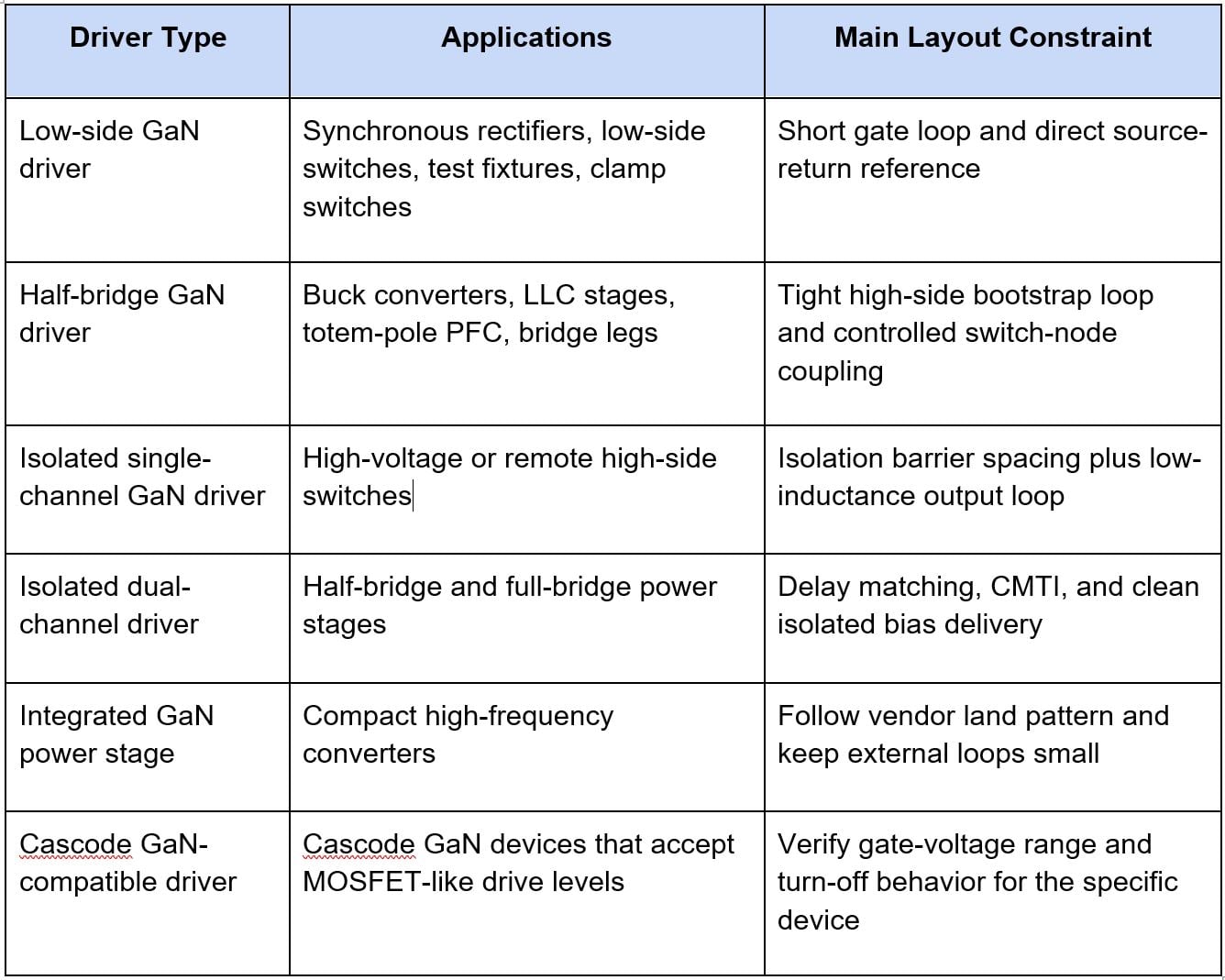
Dedicated GaN half-bridge drivers are common in compact converters because they combine level shifting, high-side drive, low-side drive, UVLO, and sometimes internal timing functions. These parts are built to tolerate fast switch-node movement, but the layout still determines whether the part sees a clean local reference. The bootstrap capacitor should sit directly between the driver bootstrap pins, and the high-side driver loop should be treated as a local floating gate-drive loop.
Isolated GaN drivers are used when the converter topology, voltage rating, or safety architecture requires galvanic isolation. In these designs, the isolation barrier and output-side gate loop have to be solved together. A good isolated driver layout can still perform poorly if the isolated output supply has a large loop area or if the driver output return shares copper with noisy power current.
Integrated GaN power stages reduce some of the layout burden because the driver and FETs are co-packaged or placed in a recommended module structure. These parts can remove parasitic inductance that would otherwise exist on the PCB. They do not eliminate PCB responsibility. The input capacitor loop, thermal vias, switch-node copper, and connections to the inductor still determine the converter’s ringing, conducted noise, and thermal behavior.
Paralleling and current sharing
Many high power systems will place FETs in parallel, and this is certainly the case with GaN devices. These devices exhibit faster switching transitions and so small parasitic differences become measurable current imbalances in parallel FETs. The typically lower noise margin on gate terminals also creates a risk of overdriving a device if another device in parallel excites a strong transient.
In switching stages, the reliability risk in static sharing is mostly driven by the total resistance along the path to the drain and source pins. The total resistance along this path is:
R(total) = RDS(on) + R(copper)
Essentially, the copper pour connection to the drain/source pins creates variations in the total path resistance seen by each GaN FET in a parallel array.
A layout that looks balanced in placement can still be electrically unbalanced if one device has a shorter (lower resistance) source-drain path. An optimal arrangement for FETs and the input voltage/current feed is sometimes best determined through a DC PDN simulation as this will help identify the total resistance along the path to the source/drain pins.
This issue with resistance along the path to the load has also been noted by Steve Sandler, managing director of Picotest.
“One of the conclusions was that the speed of the device is L/R, and L is the inductance through the power path obviously and R is the resistance of your load, and that says the more current you switch, the slower it’s going to get,” Sandler said.
This is another good reason to control the resistance along the path to the load: power delivery from each device in a paralleled GaN FET array should be coincident, and additional resistance/inductance will delay power from one of the devices arriving at the load.
Device size, capacitance and bandwidth
GaN devices should be selected for the required current and bandwidth together, not just based on voltage and current handling levels. A larger device may provide lower resistance, but it also brings higher capacitance, so we would prefer the devices to be much smaller in many fast-switching circuits. The speed limit is set by:
- Driver output impedance
- Gate-drain capacitance (Cgd)
- Power path inductance
- Load impedance
The last two items are where we get the L/R speed limit mentioned above (where R is the resistive portion of the load impedance).
The result is a tradeoff between current per device and switching speed. Higher current usually pushes the design toward larger devices or parallel devices, but this can increase capacitance and slow the transition. Smaller devices can switch faster, but the total current must be distributed across more cells. The optimal approach is to select the smallest package that provides the highest current (plus some safety margin) to ensure the power delivery speed is sufficient for the load to operate as intended.
The PCB is the last-mile obstacle
The above points regarding path inductance to the load actually tell us that the PCB is a major determinant of power delivery from GaN FET devices. The PCB determines the path inductance, which is why power supplies for high-speed digital devices and large processors demand specific design practices to ensure power integrity. With newer GaN-based supplies switching with extremely high edge rates, the output power becomes heavily influenced by the structure of the PCB.
“We can actually switch right now at 1,000 amps per nanosecond, and that’s not actually limited to the gallium nitride at all,” Sandler said. “That’s limited by the board. Now we have customers asking: can you do higher power, can you do higher power density, can you get higher speed?”
In these devices, we rely on plane pairs to transfer power to digital loads and ensure power stability up to ~1 GHz bandwidths. Above this limit, the in-package and on-chip PDN takes over as the main driver of power integrity in the digital processor. This is a more complex topic that demands its own in-depth discussion, something which we can address in a future guide.
