
Intel Foundry Direct Connect 2025 took place this week in San Jose, California, and the company reported progress on its development of advanced process technologies.
This includes the first early wafers of its 14 A process node that will rival the advanced nodes of main competitors TSMC and Samsung.
14 A process technology
Obviously, the biggest news was regarding the 14 A process node that will be the successor to Intel’s current advanced node the 18 A process. While 18 A will rival the 2 nm processor from TSMC and Samsung, 14 A will be a step to even more advanced nodes that are currently only in development from these vendors.
Intel said it has already distributed a process design kit (PDK) to customers with multiple companies expressing intent to build test chips on the 14 A process.
The 14 A processor promises a 15% to 20% performance boost and a 25% to 35% lower power consumption compared to 18 A.
18 A early wafers and expansion
Intel Foundry announced that a new performance-enhancing variant of Intel 18 A early wafers are in the fab now. Intellectual property (IP) and electronic design automation (EDA) partners are updating their offerings for the so-called 18 A-P variant.
The company said the 18 A-P variant will be the first node to support Intel’s Foveros Direct 3D with hybrid bonding interconnects for the 18 A-P variant. This will allow the company to stack dies vertically on top of its state-of-the-art processing technology. Foveros is designed to provide a capability that rivals TSMC’s hybrid bonding interconnect technology used in devices like AMD’s 3D V-cache lineup.
Advanced packaging plans
Intel Foundry expanded its packaging offerings for its 18 A and other processes including its Embedded Multi-Die Interconnect Bridge-T (EMIB-T).
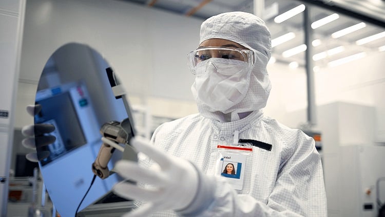 An Intel Foundry engineer holds a wafer in a clean room at its semiconductor manufacturing facility in Chandler, Arizona. Source: Intel
Expanded ecosystems
During Intel Foundry Direct Connect 2025, the company announced new alliances for chiplets and its accelerator alliance.
Synopsys Inc. and Siemens Digital Industries Software are continuing their collaboration with Intel Foundry with:
- Multiple product certifications
- Updated foundry reference flows
- Additional IC and packaging technologies
Siemens is the founding partners of the Intel Foundry Accelerator Chiplet Alliance that enables 3D IC and chiplet offerings to semiconductor verticals.
Synopsys certified its AI-driven digital and analog design flows for Intel’s 18 A process node and production-ready EDA flows for the 18 A process node with RibbonFET gate-all-around transistor architecture and commercial foundry implementation of PowerVia backside power delivery. Synopsys and Intel Foundry are also enabling EMIB-T advanced packaging technology with an EDA reference flow powered by Synopsys 3DIC compiler.
