After a rough 2025, Intel Corp. may be on the verge of getting back on track with its foundry business and is reportedly ramping up chipmaking equipment orders since the start of the year due to rising volumes.
According to a report from Anue, Intel’s volumes from its foundry business are rising more than 50% compared with last year. The uptick in equipment spending will benefit supply chain vendors KINIK Company and E&R Engineering that have close ties to the U.S. chipmaker.
E&R is a Taiwanese-based front-end wafer fabrication and back-end advanced packaging vendor. The company has a close partnership with Intel for its Raman inspection, laser processing and plasma-related tools that are currently deployed in Intel production lines and this spending will likely expand these deployments.
Taiwan’s KINIK Company’s diamond discs have been adopted by Intel since the second half of last year at Intel’s Oregon and Arizona fabs in the U.S., and in Intel’s facilities in Israel and Ireland. According to the report, the increase in spending on equipment will increase shipments of diamond disc volumes in 2026.
Attracting customers
Intel Foundry has been looking to attract major customers for its semiconductor manufacturing business with its 14A technology and advanced packaging investments are starting to gain traction.
Earlier in 2025, it was reported that Google and Amazon were in talks with intel for foundry services for custom AI chips. These would likely be used in hyperscale data centers. Intel’s advanced packaging technology were said to be one of the main reasons for companies being interested in Intel’s foundry services.
Additionally, Intel’s 14A node has seen positive indicators from various chipmakers with electronics giants like Nvidia, Apple and even rival AMD potential clients for the chipmaking process node. According to UBS Group, Intel may sign some formal foundry commitments later in 2026.
TeraFab
Early in April of 2026, Intel said it was joining Telsa Motors’ TeraFab project.
This is Elon Musk’s vision for a semiconductor manufacturing gigafab that would produce chips for Tesla vehicles and robots as well as SpaceX rockets and data centers for xAI.
Intel will help with refactor silicon technology in the proposed gigafab that is slated to begin production in 2029.
The UBS Group analysis envisioned a potential scenario where Intel combines its Ohio wafer fab with TeraFab. The move would further strengthen Intel’s foundry reputation while also giving Intel a major customer in Elon Musk’s companies.
This analysis might be closer to fruition already as Elon Musk said it will use Intel’s 14A process in the TeraFab.
"We plan to use Intel's 14A process, which is state-of-the-art and in fact not yet totally complete," Elon Musk said during Tesla's earning's call with analysts and investors. "By the time TeraFab scales up, 14A will be probably fairly mature or ready for prime time. 14A seems like the right move and we have a great relationship with Intel, a lot of respect for the CEO, the CTO and the new team there."
This likely means TeraFab will license the 14A fabrication technology from Intel and integrate it into the TeraFab. But if the companies are integrated in Ohio, that would solve many logistics issues as well.
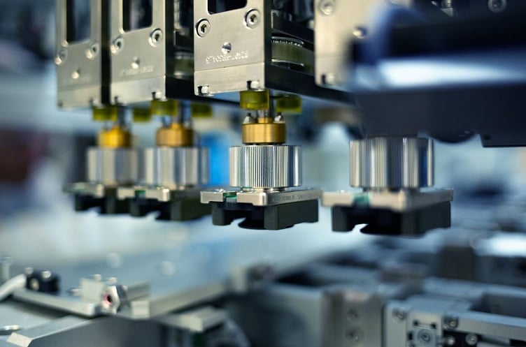
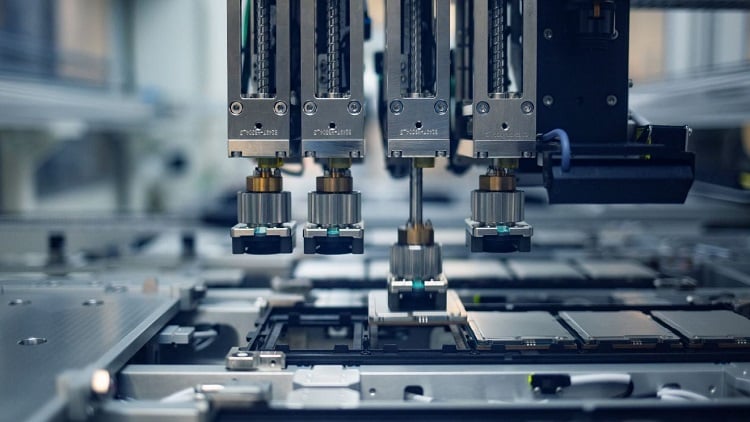 Automated final packaging systems select options for test validation at Intel’s fab in Chandler, Arizona. Advanced packaging has become a major benefit for Intel and is driving business to its foundry operations. Source: Intel
Packaging prowess
Intel has been developing its proprietary advanced packaging since 2017 with the introduction of Embedded Multi-Die Interconnect Bridge (EMIB) and later with Foveros in 2019. At Intel Direct Connect 2025, the company said it was working on packaging offerings for its 18 A and lower process nodes with its EMIB-T iteration. EMIB-T provides denser connections, better power efficiency and lower costs, Intel said.
The EMIB-T variant would support its Foveros Direct 3D with hybrid bonding interconnects. Intel said it would allow the company to stack dies vertically on top of its state-of-the-art semiconductor manufacturing technology.
Intel already uses the packages for its own products and others. These new design wins could provide higher margins and faster revenue returns compared to full-wafer deals.
Some analysts see a future where Intel packaging becomes a main part of its core business as advanced packaging becomes more important for future hyperscale AI ecosystems.
