
UCIe channels are short, dense, highly parallelized and forced into a packaging environment requiring multiple layers. The usage of multiple layers requires placement of ground to define impedance and suppress crosstalk, and yet this will impact yield and warpage, especially on organic substrates in ways that are unfamiliar to PCB designers. Since yield is related to processing step count, and thus layer count, layer reduction can be achieved with a new transmission line architecture specifically for package designs requiring moderate bandwidths.
One of the more interesting ideas discussed recently is the wallstrip transmission line. Chipletz recently presented a technical paper at this year’s DesignCon proposing this package routing style for dense die-to-die interconnects, with the channels being evaluated against UCIe requirements. Their proposed structure is aimed at one of the central package-design problems in chiplet systems: how to route a very large number of parallel signals through a short channel while keeping crosstalk, layer count and manufacturing complexity under control.
UCIe technical requirements create routing challenges
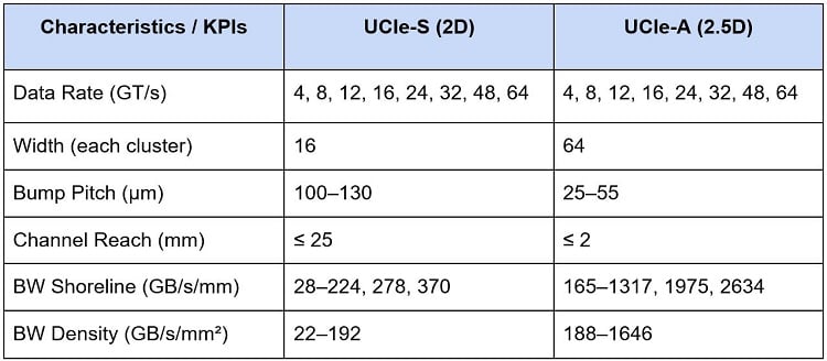
UCIe has likely emerged as the most desirable interconnect standard for die-to-die interconnects. It enables high parallelizability, large channel bandwidths, high transfer rate down to small bump pitch values. The important design targets, interface capabilities and compatibility information for the UCIe-S and UCIe-A standards are summarized below.
These numbers explain why a conventional board-level mindset does not translate cleanly into UCIe package design. The routing is a dense parallel interface in a small space, and the large number of nets to route in requires many layers when striplines are used. The high layer count comes from the need for reference planes between stripline layers to prevent layer-to-layer crosstalk.
This is why Chipletz introduced the wallstrip transmission line at this year’s DesignCon. It is an attempt to solve the actual package-level routing problem by trading routing geometry and reference structure against insertion loss, crosstalk and layer count rather than treating the channel like a scaled-down PCB interconnect.
Wallstrip transmission line overview
A wallstrip transmission line structure involves coupled signal and reference conductors mounted on their sides, (i.e., with a rectangular cross-section sitting vertically in each layer). A drawing of this structure is shown below.
By taking a stripline structure, eliminating the ground plane and placing it on its side with a nearby reference trace, the wallstrip traces would have a larger cross-section compared to a stripline in the same layer arrangement. There are two major benefits for signal integrity:
- Reduced insertion loss by reducing the skin effect loss and DC loss
- Reduced layer count through ground plane elimination
Reduced insertion loss allows for longer routes, which is beneficial in 2D packages with UCEi-S. Furthermore, it would still be possible to control the strip height by adjusting the trace density, rather than using thinner layers and smaller traces.
Because the structure eliminates ground planes between layers and instead interleaves ground traces between signal traces, the tradeoff in these designs is the re-introduction of layer-to-layer crosstalk between UCIe lanes. However, the crosstalk was found to be manageable and was outweighed by the reduced insertion loss enabled by the wallstrip structure.
According to Stephen Newberry, lead SI/PI engineer at Chipletz “…we're able to manage the crosstalk constraints within what we needed for UCIe but also provide a massive benefit on the insertion loss. And as a result, when you look at the final eye diagram time domain channel simulation results…we were ultimately able to improve the final time domain results by way of improving the insertion loss so much.”
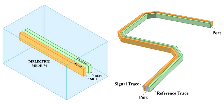 Diagram showing the structure of wallstrip transmission lines. Source: DesignCon 2026 paper by Chipletz
Yield comparison
Another factor that may not be obvious in using the wallstrip transmission line structure is the yield compared to yield on a higher layer count substrate. Because the multilayer routing strategy with wallstrip removes plane layers and repurposes that routing capacity for signals, the total number of process steps (and laminations) has been reduced.
Victor Kronberg, IC package design engineer at Chipletz, describes this as one of the fundamental challenges in package designs with highly parallelized buses.
“And part of that is the yield goes down, you multiply everything by 98% [yield], add a layer, another 98… you get kind of an exponential decrease in yield as you add more layers,” Kronberg said. “So one of the fundamental challenges is how do you reduce the layer count.”
While the signal integrity results are impressive, keeping yield high is a much more important metric for package designs supporting UCIe. By reducing the number of required layers, the leftover space can still be used to adjust the inter-layer coupling and keep crosstalk low in high-bandwidth UCIe channels.
To learn more, read the original DesignCon 2026 paper titled Enabling High-Speed Die-to-Die Interfaces with Wallstrip: A Study on Insertion Loss and Crosstalk Metrics with a Novel Transmission Line Structure.
