Researchers from the University of Texas at Austin have developed a new 3D printing method designed to make semiconductor manufacturing faster, more efficient and more environmentally friendly.
Called Holographic Metasurface Nano-Lithography (HMNL), the method will apply to semiconductors used in smartphones, robotics, aerospace and more, the university said. The goal is to create designs that were previously impossible like 3D printed capacitors that can store more energy or electronic packages that fit into unconventional spaces such as embedding AI in customized configurations that fit into robots or rockets.
“Our goal is to fundamentally change how electronics are packaged and manufactured," said Michael Cullinan, an associate professor in the Cockrell School of Engineering's Walker Department of Mechanical Engineering at University of Texas at Austin. "With HMNL, we can create complex, multimaterial structures in a single step, reducing production time from months to days.”
Metasurfaces are key
Researchers said HMNL creates a faster, more sustainable alternative to traditional electronics manufacturing.
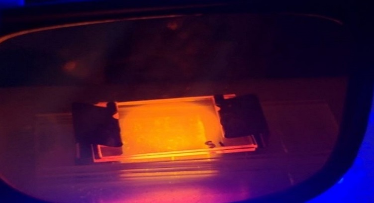
The key to this is metasurfaces, which are like optical masks capable of encoding high-density information. When exposed to light, metasurfaces create holograms for simultaneous patterning of a hybrid resin made of metal and polymer into 3D structures. The result is a process that can achieve resolutions smaller than the width of a human hair.
The process also eliminates multiple production steps and reduces material waste, minimizing the environmental footprint while accelerating prototype development.
Four prototypes
In fact, researchers created four prototypes as part of the project.
The first prototype was a commercial fan-out module for consumer devices. The second was high frequency communication and reconfigurable electronics for defense systems.
The third was an electronic package for nonplanar designs for challenging spaces. Finally, the last prototype was for active packages like a precise beam-pointing system for optical applications.
“This isn’t just about making electronics faster or cheaper; it’s about unlocking new possibilities," Cullinan said.
