
For over half a century, silicon has been the foundation of the semiconductor industry. It underpins electronics in everything from smartphones and computers to industrial automation and space technology. But as electronics continue to evolve, silicon is showing its limitations. The demand for faster processing, lower power consumption, and higher efficiency is outpacing what silicon can deliver.
Engineers are now looking beyond silicon, exploring alternative semiconductor materials that promise to push computing into the next era. These materials — ranging from Gallium Nitride (GaN) and Silicon Carbide (SiC) to emerging 2D materials like graphene and transition metal dichalcogenides (TMDs) — offer breakthroughs in speed, efficiency and power handling.
The industry is at an inflection point. As AI workloads grow, electric vehicles (EVs) demand better power efficiency and high-frequency communications expand, the shift toward new semiconductor materials is inevitable. This article explores the limitations of silicon, the emerging alternatives, and how the semiconductor landscape is evolving in real-time.
The limitations of silicon
Silicon has dominated the semiconductor industry for decades, but as technology advances, its shortcomings are becoming more apparent. Engineers are pushing silicon to its physical limits, and the challenges are mounting.
Performance bottlenecks
Silicon’s electron mobility is lower than that of alternative semiconductor materials, limiting switching speeds in transistors. As a result, high-performance computing applications — such as AI processing, 5G networks and data centers — are demanding faster alternatives.
Thermal constraints
Heat is a growing problem in modern chips. As transistor densities increase, silicon struggles to dissipate heat efficiently. This limits clock speeds and requires advanced cooling solutions, which add cost and complexity to semiconductor design.
The end of Moore’s Law
For years, the industry relied on Moore’s Law — the prediction that the number of transistors on a chip doubles roughly every two years. But as silicon-based transistors approach the atomic scale, continuing this trend becomes exponentially harder. Fabrication at sub-3 nm nodes is already facing serious technical and economic challenges.
Energy efficiency limits
Modern electronics demand better power efficiency, but silicon’s limitations make it hard to improve performance-per-watt ratios. In high-power applications — like EVs, renewable energy systems and industrial automation — silicon-based semiconductors struggle to deliver optimal efficiency.
These limitations are driving a fundamental shift in semiconductor materials. Engineers and researchers are turning to GaN, SiC and 2D materials to overcome silicon’s constraints and unlock the next wave of computing and power electronics innovation.
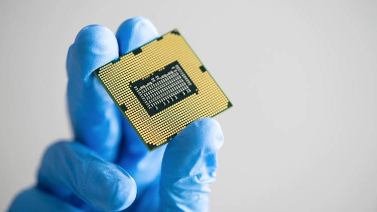 Alternative semiconductor materials like GaN and SiC as well as 2D materials like graphene and TMDs are the future of integrated circuits as silicon reaches its limit. Source: Microchip
Emerging semiconductor materials
With silicon approaching its physical and performance limits, the semiconductor industry is investing heavily in alternative materials that offer higher efficiency, faster processing, and better power handling. These new materials are set to redefine electronics across computing, communications, and power applications.
GaN is a wide-band gap semiconductor that significantly outperforms silicon in high-frequency and high-power applications.
- Higher electron mobility — GaN allows for faster switching speeds, making it ideal for RF communication, 5G infrastructure and high-speed processors.
- Superior thermal performance — GaN handles higher temperatures more efficiently, reducing heat dissipation issues common in silicon.
- Better power handling — Used in power electronics, data centers and EVs, GaN transistors improve energy efficiency and reduce system size.
Semiconductor giants like Infineon, TSMC and Navitas are ramping up GaN production to meet demand in power electronics and RF applications.
Meanwhile, SiC is another wide-bandgap material that is transforming power semiconductor design, particularly in high-voltage applications.
- High breakdown voltage — SiC can operate at higher voltages than silicon, making it perfect for EVs, industrial automation and renewable energy.
- Lower energy losses — Devices built on SiC achieve higher efficiency in power conversion, reducing heat waste and extending battery life in EVs.
- Durability — SiC semiconductors perform well in harsh environments, such as aerospace and industrial applications.
Companies like ON Semiconductor and Wolfspeed are aggressively expanding SiC manufacturing to support the next generation of high-efficiency power devices.
2D materials: The next frontier
Beyond traditional semiconductor compounds, 2D materials like graphene and transition metal dichalcogenides (TMDs) are gaining attention for their unparalleled speed and flexibility.
- Ultra-thin structure — These materials are only a few atoms thick, enabling smaller, more energy-efficient transistors.
- Superior conductivity — Graphene, for example, offers extremely high electron mobility, making it a candidate for ultra-fast computing.
- Flexible electronics — 2D materials can be integrated into wearable technology, foldable displays and next-gen sensors.
Research from the University of Minnesota and major tech companies is pushing 2D semiconductors toward real-world applications, though large-scale production remains a challenge.
Compound semiconductors
Materials like gallium arsenide (GaAs) and indium phosphide (InP) are already being used in specialized high-frequency and optical applications.
- High-speed performance — GaAs and InP offer higher electron mobility than silicon, making them ideal for 5G networks and satellite communications.
- Optoelectronics — These materials are widely used in laser diodes, photodetectors and fiber-optic communication systems.
The demand for high-speed wireless and optical computing is driving investment in compound semiconductors for telecom, defense and next-gen networking.
The race beyond silicon is already underway. As these emerging semiconductor materials become more viable, they will enable faster, more energy-efficient and more powerful electronics in the coming decade. However, despite their advantages, challenges remain in scaling these technologies for mass production and industry-wide adoption.
Challenges
The shift beyond silicon is promising, but widespread adoption of alternative semiconductor materials comes with significant hurdles. From manufacturing costs to supply chain bottlenecks, integrating these materials into mainstream semiconductor production isn’t straightforward.
Manufacturing complexity
Silicon has benefited from decades of optimization, so its fabrication is highly efficient and cost-effective. In contrast, alternative materials such as GaN and SiC require entirely different manufacturing processes that present significant challenges. Producing GaN and SiC wafers is far more expensive than silicon wafers due to lower yields and more complex fabrication methods.
Scaling production is another obstacle. While silicon manufacturing has been refined to achieve high yields, wide-bandgap materials like GaN and SiC still suffer from defects and inconsistencies during fabrication. Additionally, existing semiconductor fabs are built around silicon processing, meaning retrofitting or completely rebuilding facilities is often necessary — which adds substantial costs for chipmakers. Some progress has been made, such as TSMC’s GaN-on-Silicon approach, but achieving cost parity with silicon remains a long-term challenge.
Supply chain constraints
Unlike silicon, which is abundant and inexpensive, many alternative semiconductor materials rely on scarce or geopolitically sensitive elements. Silicon carbide production, for example, requires high-purity carbon and silicon, both of which have limited suppliers. Gallium nitride, on the other hand, depends on gallium, a byproduct of aluminum and zinc mining, which has a volatile supply chain and fluctuating availability.
Rare Earth elements are another concern. Some 2D materials and compound semiconductors, such as InP and GaAs, depend on elements that are mined and controlled by a small number of countries. This raises concerns about supply chain security, especially given the increasing global competition for semiconductor resources. Companies like Wolfspeed and Infineon are expanding domestic SiC production, but addressing these supply chain challenges will take years of investment and coordination.
Compatibility
Even if materials like GaN, SiC and graphene offer superior performance, they still need to be integrated into existing semiconductor fabrication workflows. This presents major challenges. Material defects are a significant issue — new materials often have higher defect rates in early-stage manufacturing, making it difficult to achieve consistent, high-yield production.
Hybrid approaches, such as GaN-on-silicon or 2D materials layered onto silicon chips, show promise, but they introduce new complexities in transistor design and chip architecture. Furthermore, industry-wide standardization for these materials is still in its infancy. Unlike silicon, where manufacturing techniques are highly refined and standardized, many of these new materials lack mature, scalable production processes. Overcoming these barriers will require significant investment in process development and optimization before they can be used in mass-market semiconductor production.
Cost versus performance trade-off
Adopting new semiconductor materials isn’t just a technical challenge — it’s also an economic one. While GaN and SiC deliver significant advantages in power efficiency, high-speed performance and thermal management, they are considerably more expensive per wafer compared to silicon. For industries that rely on low-cost, high-volume production — such as consumer electronics — this cost disparity slows adoption.
Similarly, 2D materials like graphene have shown exceptional properties, but they require completely new transistor architectures and fabrication techniques, which are not yet commercially viable. Even compound semiconductors like GaAs and InP, which are already used in specialized applications, remain significantly more expensive than silicon, which limits their widespread adoption.
For now, semiconductor manufacturers are prioritizing hybrid solutions — leveraging new materials where they provide the greatest performance improvements while maintaining cost-efficiency. In areas like power electronics, RF communication and AI acceleration, materials like SiC and GaN are seeing early adoption, while silicon continues to dominate in general-purpose computing.
What’s next?
Despite these challenges, semiconductor companies, governments and research institutions are heavily investing in next-generation materials. The shift beyond silicon won’t happen overnight, but the groundwork is being laid for a future where chips are faster, more efficient and no longer constrained by silicon’s physical limits. Overcoming these barriers will require a combination of new manufacturing techniques, improved supply chains and gradual industry adoption — but the direction is clear: The semiconductor industry is preparing for a post-silicon era.
About Microchip
And when the post-silicon era arrives, suppliers like Microchip USA will be right there to supply the components made with these next-gen materials — and the obsolete parts that legacy systems may still require. Microchip USA’s team of expert industry veterans has supported companies in a variety of industries — from medical and industrial to telecommunications and green energy — contact them today!
