In today’s world of wafer thinning and multilayer wafer or die bonding — with the thickness of bonded layers reduced to a mere 10% of what they used to be, making them far more brittle and susceptible to damage pre- or post-bonding — subsurface defects are more dangerous than ever. Subsurface defects that occur during the bonding or thinning process such as microcracks can be impossible to find in a production environment, leading to die yield issues or even shattered wafers resulting in the loss of hundreds of dies in an instant.
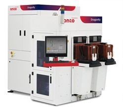 The Dragonfly G3 inspection and metrology system now offers a whole-wafer inspection capability for detecting subsurface defects. Source: Onto InnovationBut hope is on the horizon. Onto Innovation recently rolled out a new subsurface inspection capability for its well-established Dragonfly G3 submicron 2D/3D inspection and metrology platform. The new capability uses novel infrared (IR) technology and specially designed algorithms to enable the detection of yield-impacting defects at production speeds. Perhaps most importantly, inspection is not limited to the sampling of selected areas of the wafer. Users can scan an entire wafer for hidden defects, reducing the potential for scrapped wafer/die stacks and offering both improved yield and cost savings.
In a press release, Onto cites a statistic from TechInsights forecasting growth in the market for inspection products supporting wafer level packaging (WLP) — from $400 million in 2024 to more than $600 million by 2028. The stats also note that the advanced node portion of this market supporting new high bandwidth memory (HBM) technologies and advanced GPUs used in artificial intelligence (AI) applications is currently outgrowing the overall market with an annual growth rate of greater than 19%.
“Customers are demanding 100% inspection capability with production-worthy throughput,” said Mayson Brooks, vice president and general manager of Onto’s inspection business. “The Dragonfly G3 system’s new high speed IR capability delivers just that, combined with the flexibility to select from multiple objective lenses allowing customers to inspect at different magnifications for different applications and devices.”
Onto reports that it has received multiple orders for the new capability in support of HBM, advanced logic and a variety of specialty segments.
