Absolics Inc., a subsidiary of South Korean conglomerate SK Group, has broken ground on a planned $600 million investment in Covington, Georgia, where it will build glass-based semiconductors for the U.S. chip industry.
The manufacturing facility will create more than 400 jobs in Georgia and help the U.S. strengthen its supply chain by building a glass substrate-based semiconductor.
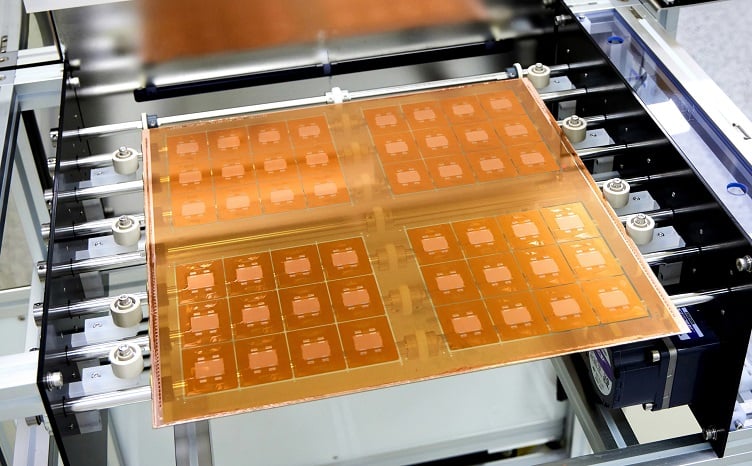
This technology features a thin layer of glass on which process and memory chips can be mounted together for new processors. The material reduces the space required for a multi-chip package so that more chips can be packed into a single device.
Breaking ground on another chip fab increases the goal of the government, vendors and trade organizations to up the domestic manufacturing of chips in the U.S. Under the newly signed CHIPS and Science Act, $52 billion in incentives and tax breaks will be given to companies looking to build new chip fabs in the U.S.
Currently, only 12% of all semiconductor manufacturing is done in the U.S. If the situation does not change, it will decline to 10% in the coming decade, according to the Semiconductor Industry Association (SIA). In 2021, 54% of semiconductors were produced by American companies.
Already, Intel Corp. has broken ground on two new fabs in Ohio due to the CHIPS Act funding and Micron Technology has pledged to build the first new memory fab in America in the last 20 years.
First to mass produce
The technology is said to be able to significantly increase the performance and energy efficiency of chipsets.
SK Group and Absolics originally developed the technology as part of a Georgia Institute of Technology research consortium and claim to be the first in the world to mass produce the material.
The inaugural product will be a thin piece of glass about 3 inches by 3 inches and will be used to package different chip components together. Absolics said processing memory and logic chips can be mounted next to each other on the glass to create the core of a computer processor.
The glass material replaces both layers of silicon that sit on top of a plastic substrate. This simplifies the manufacturing process and reduces the thickness of the package by nearly half, Absolics said.
Multi-layer ceramic capacitors (MLCC) can be embedded into the glass substrate that will free up more space on the surface of chips. Additionally, the glass substrate reduces overall power consumption by up to 50%.
Two phases
The construction of the facility in Georgia will be done in two phases. The first phase is planned for completion by the end of 2023 and the initial investment will create 140 jobs and focus on small-volume manufacturing.
As part of the first phase, Absolics expects to have an annual production capacity of 12,000 square meters.
The second phase is expected to be an additional $260 million investment and will ramp up high-volume manufacturing and will take place over the next three to five years. In the second phase, the annual production will increase to a capacity of 72,000 square meters.
