Organic field effect transistors (OFETs) are the fundamental components of flexible displays and integrated circuits. Rather than costly semiconductor materials such as silicon or metal oxides, OFETs use less expensive organic materials, enabling them to be included in large-area electronics. Conduction and operating mechanisms of OFETs as well as their applications are considered here.
Operating principles of OFETs
Field-effect transistors are composed of three major components: the source, which receives current; the gate, which regulates the output; and the drain, which discharges the transistor's current. After the input current is admitted into the source, the gate applied voltage regulates the drain output current. Current flow via an OFET is determined by the charge carriers present at the organic semiconductor and dielectric layer. As a tiny gate to source voltage is applied to the organic semiconductor, certain holes begin to pile up. As the voltage becomes more negative, several of these holes are created, growing the organic semiconductor's conductivity.
As with n-type transistors, the p-type organic transistor has two operating modes: saturation (active) and linear. Once the saturation region is reached, the drain current is equal to
I_(d(sat)) = w/2l μC_gd (V_g-V_t )^2
where w is the width of the channel, l is its length, μ represents the mobility, V_g is the voltage applied at gate, V_t represents the threshold voltage, and C_gd demonstrates the dielectric capacitance. As shown by this equation, if the source voltage exceeds the threshold, the drain current is independent of the source voltage. Moreover, the drain current rises uniformly with the gate voltage in the linear operating region, as shown by the equation:
I_(d(lin)) = w/l μC_i (V_g-V_t ) V_d
In standard semiconductors, the charge carriers move around in delocalized states. On the other hand, due to the material's low conductivity, this does not occur in OFETs, and ‘hopping’ happens in its replacement. The hopping process is the hauling of charge carriers over the orbitals of various molecules present among the acceptor and donor. Let’s get into more details.
Conduction mechanisms in OFETs
Inorganic conductors have a sea of electrons that are delocalized and work as charge carriers, facilitating the movement of current via the material. Organic compounds lack this reservoir of delocalized electrons produced by overlapping p-orbitals that form pi-bonds. The transportation of these delocalized electrons enables the conduction of electricity in organic semiconductors, where charge carriers are transported in two ways: band-like and hopping.
[Learn more about semiconductors at GlobalSpec]
In finely structured crystals, charge carriers are transported in a manner close to those of inorganic semiconductors. Such mode of transportation is inversely proportional to temperature and has been caused primarily by delocalized electrons within every molecule. In less pure or more unorganized crystals, the holes and electrons jump/hop among the molecules. This mode of transport becomes more efficient as the temperature rises. But the transmission speed is much lower than that of band-like transportation.
Applications
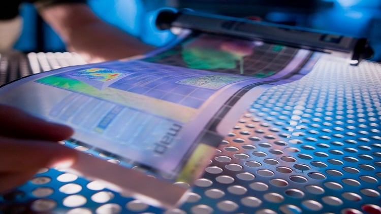
OFETs have a variety of applications that can benefit from their properties. The majority of OFET processes  Illustration of OFET architecture. Source: Creative Commons Licenseare easy to manufacture, have a low thermal budget, and are compliant with a wide variety of substrates. Such applications fuel interest in OFETs, and the long-term viability of this technology would be dictated by its capability to overcome the problems associated with these applications.
Field-driven display components like liquid crystals are usually matrixed to achieve massive panel sizes while maintaining a reasonable number of external connections. OFETs are an ideal solution for this category of applications. Moreover, OFETs exhibit many of the same properties as amorphous silicon (a-Si) LCDs, but with a much larger thermal budget. Due to the lower thermal budget, manufacturing on plastic sheet, glass and metal foils is possible. Apart from the possible cost savings associated with simpler processing through printing or evaporation, OFETs can also be used in current drive applications, providing lower bias stress as compared to a-Si transistors manufactured at temperatures lower than 200° C.
OFETs are well adapted to switching and amplifying mechanical actuations due to their flexible mechanical properties and big size. Flexible and big backplanes made possible by OFET technology will also support image sensing systems, all of which may benefit from either mechanical flexibility or large surface features. Currently, flexible, lightweight, large-area sheet image scanners deploying high-quality organic transistors are being successfully manufactured on plastic films. OFETs may also be used in ultra-low-cost logic components and RFID tags. With all-printed and flexible printed circuits, the OFET would significantly disrupt the existing RFID market, displacing barcode technology and serving as a security tag for passports and banknotes.
Conclusion
Organic semiconductors have been used in a wide variety of electronic and optoelectronic applications due to their compatibility and chemical flexibility with a wide variety of processing methods. The OFET is one such module composed of a conducting polymer that serves as a drain/source, which is placed on a polyester-based polymeric layer, a phenylsilane-based insulating polymer for manufacturing the gate dielectric, a semiconductor polymer and a flexible polymer-based substrate. The OFETs are enormously appealing technologically and are being used in a variety of applications ranging from displays to RFID tags.
