Testing is a crucial component in printed circuit board (PCB) assembly for detecting defects, faults and errors. Various electronics test fixtures can be employed to test contact points on circuit boards. Here is a closer look.
 Electronics test fixture. Source: Advanced Energy Industries Inc
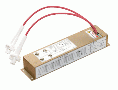
Electronics test fixtures can be used to test:
- daughter cards
- flex circuits
- liquid crystal displays (LCDs)
- loop-back boards
- multi-chip modules
- optical packages
- printed circuit boards (PCBs)
- radio frequency (RF) modules
- hybrid boards
Computer-controlled testing and measurement equipment allows for automated testing with minimal human interaction. Automated test equipment (ATE) can be used to test integrated circuits (ICs) when attached to an interface between the IC and a device under test (DUT) board. As a rule, DUT boards are designed to meet all of the mechanical and electrical requirements of both IC chips and electronics test fixtures.
 Automated test equipment. Source: B&K Precision Corporation
- Manufacturing defect analyzers (MDAs), or analog circuit testers, are used to identify and locate defects such as shorts and missing components. Because the unit under test (UUT) is powered-down, however, MDAs are not designed for testing digital ICs. MDAs operate on the premise that the IC is functional, and are much less expensive than other test options.
- In-circuit analyzers, or digital circuit testers, are used for testing components that are part of a board assembly. Because the UUT is powered-up or hot, the components under test are considered to be in a circuit. In-circuit testers (ICTs) are very powerful but are limited due to the high density of tracks and components in most current designs. The pins for contact must be placed very accurately in order to make good contact.
- Functional analyzers, or emulators, are electronics test fixtures that simulate an operating environment. They are used for testing boards against their functional specifications. Functional automatic test equipment (FATE) is unpopular due to the equipment not being able to keep up with the increasing speed of boards; this causes a lag between the board under test and the manufacturing process.
In a bed-of-nails (BON) configuration, each circuit net on the board is connected to the tester, typically with one nail per net. The pins are aligned to make contact with test points on a printed circuit board. They are also connected to a measuring unit by wires. When the DUT is pressed against the BON, contact is made simultaneously with hundreds or thousands of individual test points. BONs typically require a vacuum or air source to ensure hold-down force is provided.
The flying probe system uses a low number of moving probes rather than the high number of fixed probes in the BON. Test times may be slower due to probe movements, but the method has compensating benefits. In practice, a flying probe can provide close to 100% test coverage on a board with thousands of nets of passive components and hundreds of digital devices. It is best used with assembled boards for new product introduction.
Above: Flying probe testing. Source: Nexlogic PCB Design / CC BY-SA 4.0
Optical inspection methods include scanning probe microscopes that reveal surface defects. Optical inspections do not need test fixtures and require no electrical sources or measurements. Automated optical inspection (AOI) is helpful when placed at the end of a line producing soldered boards. Here it can quickly locate production problems such as solder defects and incorrect component orientation. The set up time can be tedious, but once set the system can process boards efficiently, making it ideal for high volume processing. Automated X-ray inspection (AXI) is similar to optical inspection. It can look through IC packages to examine solder joints.
The chart below compares the major defect detection capabilities between automated optical inspection, automated X-ray inspection and in-circuit testing.
| DEFECT TYPE | AOI | AXI | ICT |
|---|---|---|---|
|
Soldering defects | |||
| Open circuits | Y | Y | Y |
| Solder bridges | Y | Y | Y |
| Solder shorts | Y | Y | Y |
| Insufficient solder | Y* | Y | N |
| Solder void | N | Y | N |
| Excess solder | Y | Y | N |
| Solder quality | N | Y | N |
|
Component defects | |||
| Lifted lead | Y | Y | Y |
| Missing component | Y | Y | Y |
| Misaligned or misplaced component | Y | Y | Y |
| Incorrect component value | N | N | Y |
| Faulty component | N | N | Y |
|
BGA and CSP defects | |||
| BGA shorts | N | Y | Y |
| BGA open circuit connections | N | Y | Y |
*Note: AOI cannot detect an insufficient solder defect on heel of joint. Source: Radio Electronics
Standards
Automated test equipment must adhere to several national and international standards. The U.S. Air Force publishes standardized policy for ATLAS high order language (HOL) for automatic test equipment as well as a policy for modular ATE. British Defense Standards have specifications for automatic test equipment and general purpose ATE date requirements.
More information
For more information on all types of electrical and electronic test equipment, visit our dedicated section on Engineering360. It includes links to specification guides, as well as listings of manufacturers, distributors and service providers.
