The push for smaller and lower power devices has created a need for new fundamental printed circuit board (PCB) technology. While many new PCB technologies are still at the research stage, expect some advances in the future as they go from research to production.
To talk about future PCB technology it is important to understand where the existing technology is.
Traditional PCBs are most often made of fiberglass with metal layers. One existing change to that is flexible and rigid-flexible PCBs. These use a flexible substrate material and can be used as wiring or have components soldered on them. The use of rigid-flexible PCBs allows the combination of a rigid PCB that converts to a flexible material without any connectors. The flexible nature allows designers the freedom to fold or roll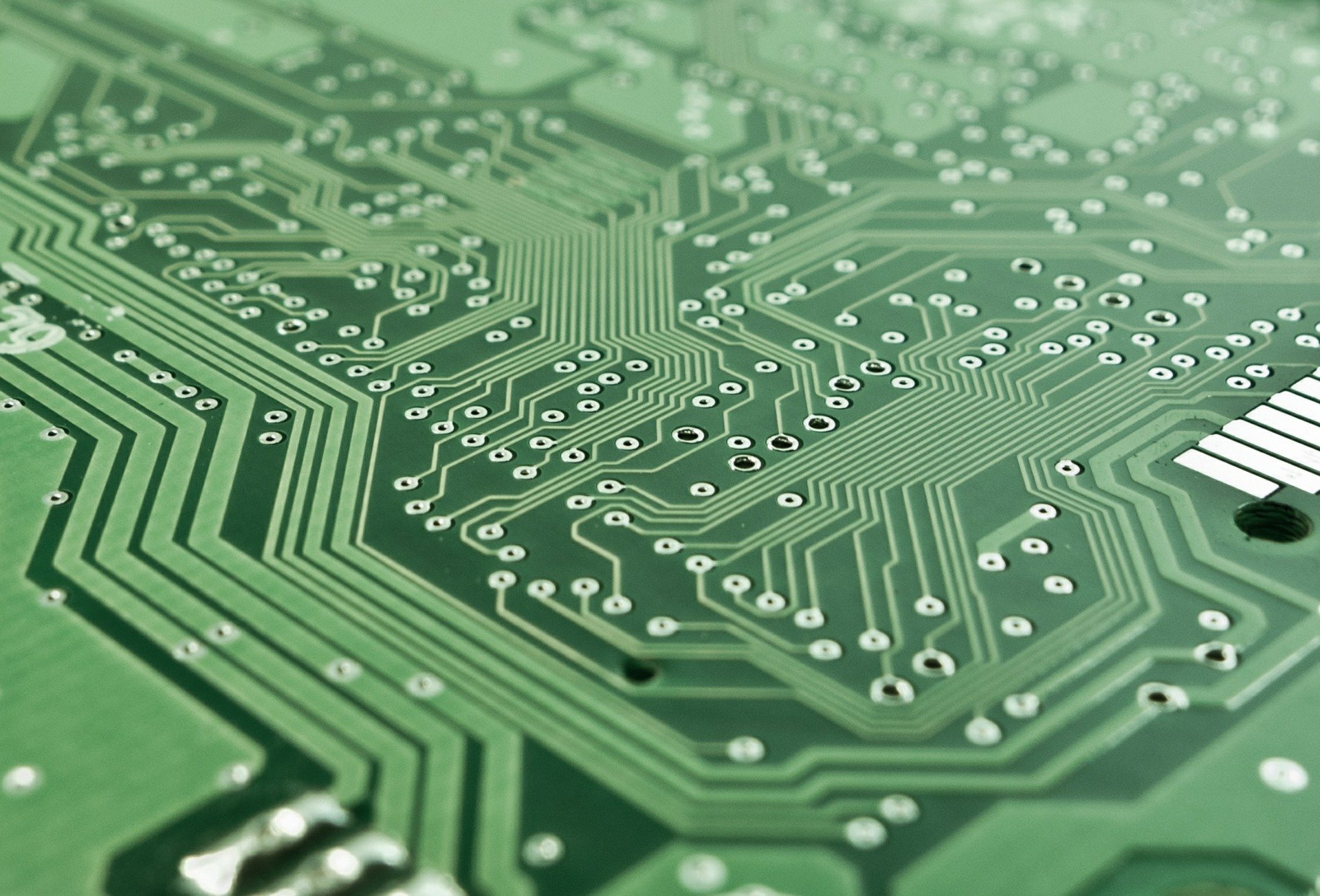 a circuit board to fit in a specific size or packaging.
Another existing technology is the use of many layers. Stacking thin layers of circuit connections allows for easier routing and more compact spacing of components. This relies on a number of thin PCBs that are sandwiched and bonded.
A future possibility is embedding some components into the board. This is already done to a minor extent with building inductors and capacitors into the PCB. Inductors are made with a coil of wire, which can be printed directly in the shape of a spiral. The practicality of this method depends on the inductance value required. Capacitors are two closely spaced conductor plates; this can also be achieved with a board of two or more layers. Once again the value and accuracy of the capacitance will impact whether or not this method is practical. Resistors are composed of a material such as carbon or wire that resists the flow of electricity. On a PCB this can be achieved by utilizing very thin and long traces of painting carbon or other high resistance material. With this method, the tolerance of the resistor may not be very high.
These methods are done today to a limited extent, along with a few other similar passive components such as a fuse, switch, motor coils and antenna. Often the limitations of these methods make them desirable only for specific applications.
The next step is to build components into the PCB but not by etching them like the current practice. The advent of 3D printing is one potential path, where the circuit is printed instead of etched and components are placed and bonded during the machining. With current technology, the etching equipment of building a multi-layer board doesn’t typically have the ability to place and solder components. With the existing process, the PCB fabrication and part placement and soldering often occur at different facilities, making them difficult to integrate. 3D printing circuit boards is in its infancy and used for prototypes. It often uses a solder-like material which would allow for easy connection of components. There is potential for further integration of the PCB fab and manufacturing companies enabling this technology with new or modified machines.
These components are passive but active components could potentially also be embedded. Another common practice for products manufactured in large volume is to put the silicon die directly on the PCB and put a blob of epoxy on top to protect it. This method is often called a glob top and adds expense on the manufacturing side but reduces the part cost. Practices like these, although already done, could become more widespread. In the future, it may be possible to place a silicon die between layers further reducing the circuit size. This is not as simple as soldering; wire bonding to a silicon die requires more precise and expensive equipment. Heat may also be an issue depending on the chip.
As the push to reduce sizes of circuits becomes increasingly important and the technology available to do so matures, the use of embedded components will need to increase. This will mostly rely on high volume products pushing the development of the equipment and processes.
