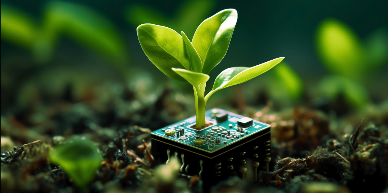
The University of California, Berkeley, states that after many years of employment, flame-retardant fiberglass-reinforced epoxy resin (FR4) remains the market-standard material for printed circuit boards (PCBs). For years, its dielectric capabilities have supported electronics engineers as they economically design equipment that is resistant to high temperatures. However, sustainability initiatives require the sector to reevaluate how it sources materials and assembles and disposes of PCBs. What options do professionals have to make greener tech?
Sustainability concerns with FR4 and PCB design
FR4 substrates have become a mainstay because they are a mature technology. Specs, compliance frameworks and optimal applications are well-defined to forge compact, multilayered boards. However, manufacturers seal their assemblies with two problematic materials — glass and cured epoxy. These are a concern because they do not biodegrade, require fossil fuels to produce and release pollutants like volatile organic compounds during processing.
 Source: Cala Serrano/Adobe Stock
Flame retardants are also typically brominated, making them an intensely toxic compound to interact with. They make FR4 even more unsustainable because they pollute the air, soil and water, which enter the food chain. If dangerous compounds reach ranch animals and fish, they could contaminate humans through trophic transfer.
PCBs contain many layers of glass fiber cured in hard plastics. This is intentional to make electronics more durable. However, this makes disassembling a PCB at the end of its life cycle nearly impossible because of the sealant’s toughness and molding to the PCB’s other components. Only 20% of PCBs are collected for attempted recycling. Additionally, concerns about glass scarcity because of sand shortages and reluctance to drill for polymer raw materials make matters more complex from an environmental perspective.
PCB designs have other climate considerations to make outside of using FR4, including:
● Mining impacts from extracting metals like gold, aluminum and iron
● Lack of component recovery and circularity
● Nonmodular structures
● Minimal repairability
● High energy consumption during manufacturing
● Resource-intensive semiconductor fabrication and forgoing wet etching for dry methods
Sustainable design alternatives
Eco-aware design substitutes have an opportunity to overcome conventional methods’ shortcomings. For example, FR4 insulation limits could have higher thresholds, and signal integrity needs to be enhanced to be more adaptable to high-frequency deployments. Curated laminates have a higher dissipation factor. Are there sustainable design choices considering these obstacles?
Vitrimer
The University of Washington is researching the potential of vitrimer, a recently introduced polymer. It is moldable yet sturdy when stable, making PCBs equally rigid and flexible. This is more sustainable than epoxy because it is simple to change its molecular structure for easy retrieval. Vitrimer forms new bonds under heat, and engineers can force the molecules to rearrange themselves into optimal shapes. It then reveals access to the removable components. Vitrimer also degrades quite slowly, so multiple restructurings should have little to no negative impact on the PCB.
Biomaterials
Compostable and bio-based PCBs are another new research domain. Options include chitosan, cellulose and even wood. Processing would not require polluting wastewater, and biomaterials are inherently renewable. However, all-natural materials need more development and investments to become as reputable as classic design structures. Current obstacles include minimizing flammability and arc resistance, among others.
3D printing
Many raw materials can be processed and assembled with additive manufacturing. Electronics engineers often produce many prototypes in the R&D process, inevitably leading to prototype materials going to waste. Using eco-friendly 3D printing materials allows for guilt-free modeling in early production phases. Incorporating 3D printers encourages lean manufacturing principles, optimizing operations by slashing creation times and producing less waste. Modern research has validated the potential for materials like organically made polylactides in developing Class 2 and 3 PCBs.
However, they are not commercially viable because no alternative matches the performance and quality of standard PCBs. This hints at the most prominent obstacle in 3D printed circuit board substrates: manufacturing disappointments caused by material inadequacies. Polymer- and ceramic-based substrates have varying conductivity, thermal management and dielectric potential but must match the power and consistency of materials like copper. If electronics designers craft a suitable design despite the lack of 3D printed PCB standardization, they will likely still encounter issues like persistent delamination signaling poor layer adhesion.
PCB recycling infrastructure
Commercializing sustainable PCB designs is critical for the industry’s future. However, engineers must remain focused on remediating and repurposing wasted materials. Australia alone generates 25 kilotons of PCB e-waste yearly, leading to chemical leaching and wildlife habitat destruction.
Research and input-output modeling have attempted to document precious metal and component recovery efforts for this type of e-waste. This gives manufacturers the option to reduce sourcing new gold and copper when countless tons already exist on the market, which could be recoverable with a better focus on recyclability.
This should help regulators define policy, incentivizing or enforcing participation in expanded PCB recycling infrastructure. For programs to work, they must include a comprehensive structure, including organization, preprocessing, processing and redistribution plans.
Preprocessing includes disassembling PCBs, separating constituent parts and sizing everything in their subcategories to assist advanced recyclers with processing. The effectiveness of this stage relies on how modular passive parts and integrated circuits are. When PCBs may include many other components, including transistors, diodes, relay switches and more, this must be as accurate as possible.
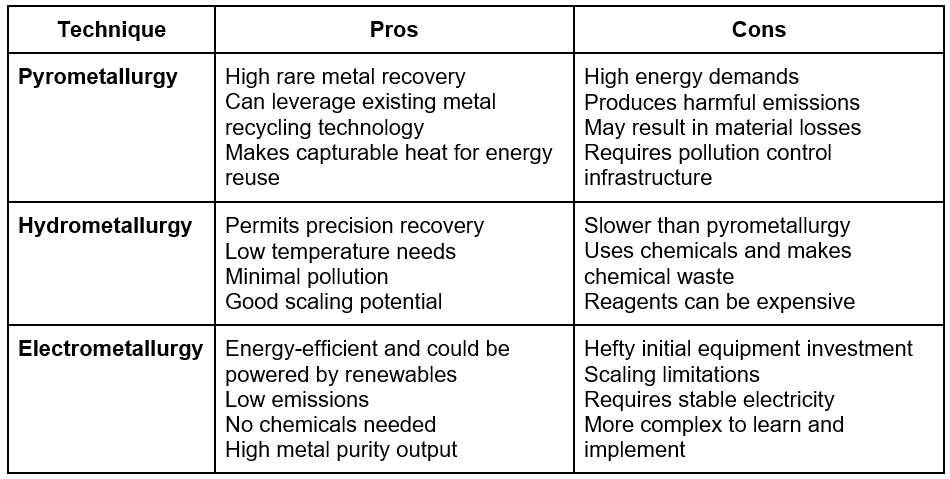
Mechanical and chemical processes have various pros and cons. Some may have lower recycling rates than others or have less precision. These strategies are a few approaches to closing both gaps with more sustainable methods:
● Pyrometallurgy: Uses heat to cause a chemical reaction to separate components
● Hydrometallurgy: Leverages an aqueous solution to filter parts
● Electrometallurgy: Uses electrochemical processes, typically in an electrolytic cell
What are the pros and cons of each method?
Collection and distribution optimization requires third-party partnerships to expand pickup and drop-off points. It also demands clear communications so PCB and e-waste acquisitions teams know how to transport materials to recyclers in ways leading to the highest rate of recyclability.
PCBs of a greener future
Eco-friendly PCB makers and electronics engineers must phase out FR4 and other unsustainable practices to meet future demands. It is vital to divert attention to expanding recycling infrastructure and developing research. The current state of the market is in flux but making headway toward greener practices.
There will be more to come in sustainable PCB development in addition to the mentioned trials. Tests are using more polylactic acids and mixing them with organic resources like flax textiles for improved life cycle analyses. Acid leaching may recover metals. The possibilities are endless.
Projections in sustainable electronics manufacturing anticipate growth in the next decade. This signals the potential for these ideas to become commercialized soon.
About the author
Ellie Gabel is a science writer specializing in astronomy and environmental science and is the associate editor of Revolutionized. Ellie's love of science stems from reading Richard Dawkins books and her favorite science magazines as a child, where she fell in love with the experiments included in each edition.
