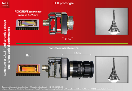
 Leti's prototype with PIXCURVE technology compared to a commercial reference: performance improves, while size, complexity and cost are reduced. Source: Leti
Leti, a research institute at CEA Tech based in Grenoble, France, has developed a new curving technology for optical sensors and micro-displays that improves performance, enhances field of view and compensates for aberrations in optical applications.
The technology curves components such as complementary metal–oxide–semiconductor (CMOS) imagers and charged-couple device (CCD) imagers for mobile phones, cameras, telescopes, medical-imaging tools and industrial-control equipment. Other uses include IR sensors for astronomy, defense, drones and micro-displays for automotive applications, augmented reality and virtual reality.
Leti’s fully functional prototype of its PIXCURVE technology was presented in the paper, “Curved Sensors for Compact High-Resolution Wide Field Designs: Prototype Demonstration and Optical Characterization,” at Photonics West 2018, San Francisco, in collaboration with LAM (Laboratoire d’Astrophysique de Marseille).
A demonstration of PIXCURVE at the event was based on a 1/1.8 in. format, 1.3-million-pixel CMOS image sensor. The standard sensor structure consists of a 7.74 x 8.12 mm silicon die glued on a ceramic package. Electrical connections are wire bonded from the die to the package surface and, then, to the interconnection board. A glass cover is placed on top for mechanical protection.
Leti’s technology uses a grinding process to get the sensor below 100µm thick, which makes it mechanically flexible. It is then glued onto a curved substrate, which determines its final shape. A wire bonding process developed for electrical connections is used to prevent damages on the thinned dies. This process is compatible with any sensor size and with large-scale manufacturing methods.
