ON Semiconductor has launched a CMOS image sensor platform that brings new levels of performance and 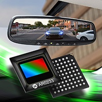 (SOurce: ON Semiconductor)image quality to automotive applications such as advanced driver-assistance systems (ADAS), mirror replacement, rear and surround view systems and autonomous driving. The Hayabusa™ platform features a 3.0-micron backside illuminated pixel design that delivers a charge capacity of 100,000 electrons, the highest in the industry, with other key automotive features such as simultaneous on-chip high dynamic range (HDR) with LED flicker mitigation (LFM), plus real-time functional safety and automotive grade qualification.
“The Hayabusa family enables automakers to meet the evolving standards for ADAS such as European NCAP 2020, and offers next-generation features such as electronic mirrors and high-resolution surround view systems with anti-flicker technology. The scalable approach of the sensors from ½” to ¼” optical sizes reduces customer development time and effort for multiple car platforms, giving them a time-to-market advantage,” said Ross Jatou, VP and GM of the Automotive Solutions Division at ON Semiconductor.
The high charge capacity of this pixel design enables every device in the Hayabusa family to deliver Super-Exposure capability, which results in 120-decibel (dB) HDR images with LFM for high image fidelity in the most challenging scenes without sacrificing low-light sensitivity. The simultaneous HDR and LFM capability is especially important in enhancing safety, as it ensures that all objects and potential hazards can be identified in both very dark and very bright areas of the scene. With the widespread use of LEDs for front and rear lighting, as well as traffic signs, the LFM capability of the platform makes certain that pulsed light sources do not appear to flicker, which can lead to driver distraction or, in the case of front facing ADAS, the misinterpretation of a scene by machine vision algorithms.
The Hayabusa product family also features real-time, ISO26262-compliant functional safety capabilities to alert the system processor if the sensor has any issues or potential errors. These features enable system designs rated up to ASIL-C. The real-time capability enables errors to be identified immediately rather than waiting for the full image to be transferred to the processor and then waiting for image analysis. This faster response time means the system processor can take immediate action to remedy the issue, which is crucial when considering that a vehicle moving on a freeway easily covers 100 feet in less than one second.
The first product in this family, the 2.6 megapixel (MP) AR0233 CMOS image sensor, is capable of running at 60 fps while simultaneously delivering ultra-high dynamic range and LED flicker mitigation along with all of the Hayabusa platform features.
