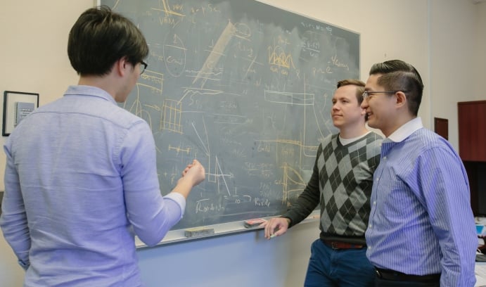
 Researchers Guosong Zeng, with Brandon Krick and Nelson Tansu (from left). Studies found that GaN’s wear resistance exceeds sapphire and approaches that of diamonds. Source: Christa Neu/Lehigh UniversityGallium nitride’s (GaN's) list of virtues as a semiconducting material is impressive. It is optoelectronic and mechanical properties make it ideal for a variety of applications, including light-emitting diodes (LEDs), high-temperature transistors, sensors and even biocompatible electronic implants.
Now researchers at Lehigh University have discovered yet another, and until now unknown, virtue: GaN’s toughness approaches that of diamonds, the hardest known material. That wear resistance promises to open up the material’s applications in touchscreens, space vehicles and radio-frequency microelectromechanical systems (RF MEMS)—all of which require high-speed, high-vibration technology.
The electronic and optical properties of GaN have been studied extensively for years, but Lehigh University researchers believe they are the first to examine its tribological properties, that is, its resistance to the mechanical wear imposed by reciprocated sliding.
As explained by the researchers, wear rate is expressed in negative cubic millimeters of Newton meters, or Nm. The rate for chalk, which has virtually no wear resistance, is on the order of 10-2 mm3/Nm. On the other end of the spectrum, the rate for diamonds is between 10-9 and 10-10. The rate for GaN ranged from 10-7 to 10-9, approaching the wear resistance of diamonds and three to five orders of magnitude more resistant than silicon at 10-4.
Several factors were cited for the variance in wear resistance ratings, including environmental conditions, especially humidity. As humidity was increased in the experiment, the wear rate of GaN also increased, researchers noted.
The group’s discovery could have a dramatic effect on the electronic and digital device industries, said Nelson Tansu, professor in the Department of Electrical and Computer Engineering, and director of the university’s Center for Photonics and Nanoelectronics. In a device such as a smartphone, the electronic components are housed underneath a protective coating of glass or sapphire, he noted. This poses potential compatibility problems, which could be avoided by using GaN.
“The wear resistance of GaN,” he said, “gives us the opportunity to replace the multiple layers in a typical semiconductor device with one layer made of a material that has excellent optical and electrical properties and is wear-resistant as well.
“Using GaN, you can build an entire device in one platform without multiple layers of technologies. You can integrate electronics, light sensors and light emitters and still have a mechanically robust device. This will open up a new paradigm for designing devices. And because GaN can be made very thin and still strong, it will accelerate the move to flexible electronics.”
