Sometimes, when a technology has existed for a long time, people regard it like an old shoe—useful and reliable but no longer something that merits particular attention. The initial impetus for the development of IEEE standard 1149.1—boundary scan for electronics manufacturing—stemmed from designers’ reluctance to adopt quality and testability as valid requirements for both chips and printed circuit boards (PCBs). In the 25 years since its adoption, many engineers have recognized its power to achieve visibility into the logic states on even complex PCBs, yet still neglect to make necessary decisions during design that take maximum advantage of that power to make their lives easier and improve board quality at the same time. Circuit complexity and the ever-increasing number and length of boundary-scan chains have encouraged specific modifications to original design-for-testability guidelines that engineers once regarded as overkill.
Among the recommendations:
In addition to the mandatory (test-data in [TDI], test-data out [TDO], test clock [TCK], test-mode select [TMS]) and optional (test reset [TRST]) pins in a test header at the board edge, conventional wisdom recommends selecting chips wherever possible that contain their own test-access ports (TAPs) with adjacent memory elements to buffer TDI and TDO. Keeping the buffers for the input signals as close as possible to the board’s boundary-scan header reduces noise and skew between TCK and other signals. Daisy-chaining the test ports together from the test header’s TDI to the TDI of the first chip in the chain, then from that chip’s TDO to the next’s TDI all the way out to the header’s TDO, creates a single boundary-scan chain for the scannable board logic.
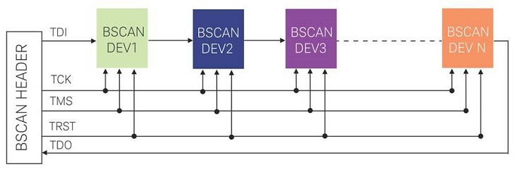 A single boundary-scan chain that encompasses all scannable logic. (Image source: Keysight Technologies)
Some boundary-scan experts recommend a 22 Ω resistor between the board header TDI and the TDI on the first device, and another between the last device’s TDO and the corresponding board header pin. If the board design requires long signal paths, choose buffers that feature high drive strength. The design should distribute signals for TMS, TCK and TRST pins through fanouts to no more than eight devices per output node. If the boards include devices still in development, stay in contact with the vendors to ensure that you can incorporate any changes in device specifications caused by issues that emerge before you receive the finished products.
To ensure stability of devices in their functional states by default, insert resistors of any value between 1 kΩ and 4.7 kΩ on the five board-header boundary-scan signal lines. Pull TDI, TMS and TDO up to Vcc and pull TCK and (optional) TRST down to ground.
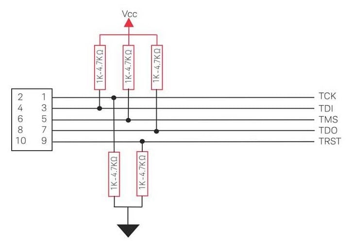 ull-up and pull-down resistors on the boundary-scan signal lines maintain device stability. (Image source: Keysight Technologies)
Exercising the full chain in a single step permits a short test to make a pass/fail decision. Appropriate as a first-pass during production where you expect few failures, most of which resemble problems uncovered during development, this approach may prove inadequate for identifying and correcting anomalies you had not anticipated. Addressing those failures requires more detailed analysis.
A resistor or jumper between one device’s TDI and TDO effectively bypasses that device. The same principle allows bypassing several devices of the same type, such as multiple memories or identical application-specific ICs (ASICs). Isolating one or more devices in the chain can verify their behavior during board development or while debugging the test program before ramping up for full production. In production, if the chain fails, using the jumpers to bypass some devices isolates individual logic segments in-line or at a repair station to pinpoint the cause.
For boards containing several programmable devices, group them together at either end of the chain to allow the board header to perform programming as well as boundary-scan testing. However, to further enhance board stability during testing, exclude programmable devices or ASICs that specifically handle power management from the boundary-scan loop.
The source document contains additional recommendations for multi-board configurations and other situations you may encounter.
Source: http://literature.cdn.keysight.com/litweb/pdf/5992-1222EN.pdf?id=2694201
