The ECP5 Versa development kit by Lattice Semiconductor accelerates prototyping and testing of connectivity designs targeting small cells, microservers, broadband access and industrial video applications. The family’s low power consumption, small form factor and low cost enable design engineers to rapidly add features and functions that complement those delivered by ASICs and ASSPs.
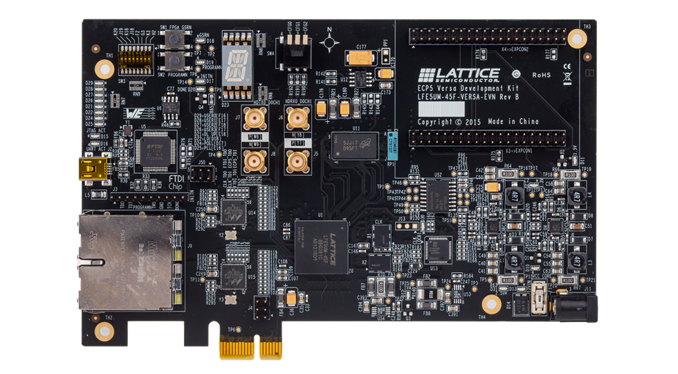 ECP5 Versa Development Board Top View. Source: Latticesemi.comThe ECP5 family’s architecture is optimized to deliver the best value below 100K LUTs, while adding features such as support for soft error correction and small form factor packages across all densities. Achieving 40% lower cost than competing solutions, optimizations include small LUT4 based logic slices with enhanced routing architecture, dual-channel SERDES to save silicon real estate and enhanced DSP blocks for up to 4x resource improvements.
The kit lets customers evaluate the connectivity performance of the ECP5 FPGA with standards such as PCI Express, Gigabit Ethernet, DDR3 and generic SERDES. The company also offers several proof-of-concept demos with the kit that can help customers accelerate prototyping and testing of designs.
Additionally, the ECP5 Versa development kit includes the Lattice Diamond Design Software offering a complete suite of FPGA design tools with an easy-to-use interface, efficient design flow free of charge to all users purchasing the board.
The development kit is available direct from the company at a limited promotional price of $99.
Related Links:
