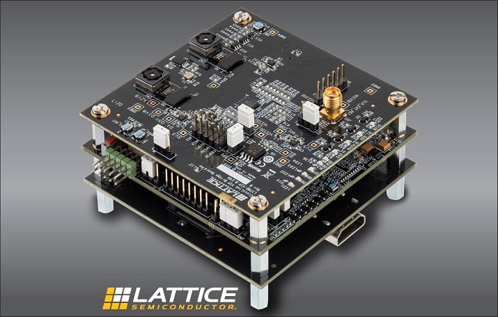
 Lattice’s embedded vision development kit. Image credit: Lattice
Lattice Semiconductor Corp. has introduced an embedded vision development kit for mobile applications that require a low cost and low power image processing architecture.
The kit combines Lattice’s field programmable gate array (FPGA) ASSP and programmable ASSP (pASSP) products in a single, modular platform in order to provide the flexibility and energy efficiency for embedded vision applications in industrial, automotive and consumer markets.
The development kit is designed to accelerate the development of next-generation intelligent, vision-enabled devices by combining the CrossLink pASSP mobile bridging device, ECP5 low power, small form factor FPGA, along with a high resolution HDMI ASSP.
The CrossLink input board includes a dual-camera HD image sensors with support for MIPI CSI-2 interface that eliminates the need for external video sources. The ECP5 based board enables low-power pre/post processing and includes support for HD image signal processing intellectual property from Helion Vision. The kit also includes a NanoVesta connector to support external image sensor video inputs.
