Intel has provided some details of its first microprocessor implemented on the company's 14nm FinFET manufacturing process – the Broadwell-Y otherwise known as Core-M. The processor is expected to be essentially a shrink of the previous Haswell-Y on 22nm FinFET process and the main conclusion Intel draws is that the move to a finer geometry will more than halve power consumption.
The processor is aimed at tablet and netbook computers and is expected to be enable then to be thinner, cooler and with the potential to be fan-less. This is something the previous generation of Haswell processors for mobile applications on the 22nm FinFET process was unable to support.
Some commentators at the time put this down to disappointing performance of the trapezoidal-profile fins in the 22nm FinFET process, which produced processors that still had substantial power consumption despite reduced clock frequencies and various power-down modes of operation. In its presentation Intel claims that in Broadwell and the 14nm FinFET process it has improved the structure of the fins.
Whether the engineering to improve the fin shape and reduce power consumption has been the reason for delays for the introduction of the 14nm FinFET process and Broadwell-Y/Core-M processor is not clear – but delays there have been.
Intel CEO Brian Krzanich announced a delay in the launch of product and process in October 2013 due to "technical issues"; problems in driving down defect density and bring up yield (see Intel Delays 14-nm Broadwell, Posts Mixed Q3). What was going to be a one-quarter delay appears to have changed into a year as products with 14nm Broadwell processor inside are now expected to ship in 4Q14 rather than 4Q13. Nonetheless, Intel is the first chip company to make chips on such as miniature logic technology.
Intel said in its presentation that the Core-M would halve power consumption while providing better performance than Haswell-Y. Haswell-Y is a similar microprocessor that was implemented in 22nm FinFET manufacturing process technology. Other benefits to come from the adoption of the 14nm FinFET process include half the package footprint and a 30 percent thinner package with idle power reduced by 60 percent.
"Intel's 14nm technology is now qualified and in volume production," Intel said attributing the comment to Mark Bohr, Intel senior fellow, also claiming that the 14nm FinFET process has industry-leading performance in terms of power, density and cost per transistor. Intel has also added a second-generation fully integrated voltage regulation circuit (FIVR) that improves efficiency at lower voltages.
Fins ain't what they used to be
The fin pitch of the transistor has been reduced from 60nm in the 22nm process to 42nm in the 14nm process while the interconnect pitch has decreased from 80nm to 52nm, respectively.
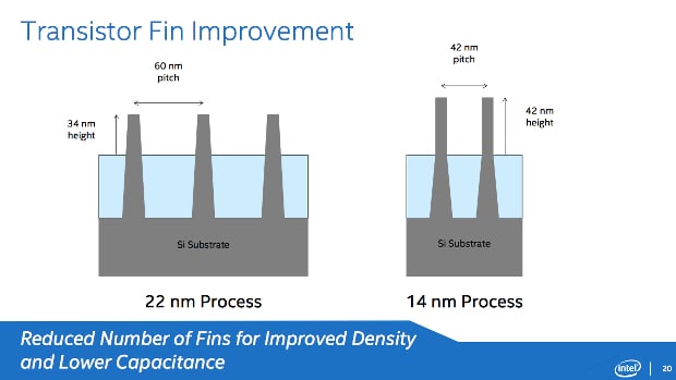
A reduced number of fins on a finer pitch are source of 14nm FinFET improvements. Source: Intel.
In addition Intel claims it has improved the fin shape in this second generation of its process, producing taller thinner fins that are 42nm tall for increased drive current and performance. While Intel shows the fins in idealized form as perfectly rectangular a cross-sectional diagram shows a more complex attenuated and rounded structure.
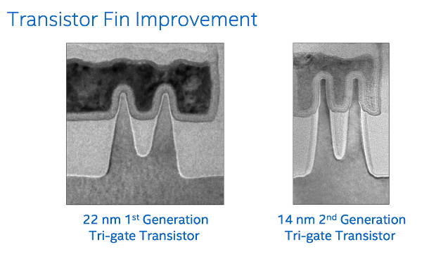
Are those 14nm fins more rectangular? They are definitely smaller. Source: Intel.
When benchmarked for an SRAM cell Intel reckons the use of 14nm manufacturing process produces an area just 54 percent that of the 22nm SRAM; 0.0588 square microns versus 0.108 square microns when based on SRAM deployed in processors.
Intel made the point that it will be shipping its second-generation FinFET generation before rival vendors such as Taiwan Semiconductor Manufacturing Co. Ltd. and Samsung are shipping their first generation. Intel said it has produced its 14nm FinFET, which is denser and earlier than what others call 16nm or 14nm.
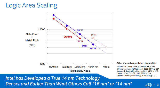
Intel plots a straight-line for its manufacturing process progress. Source: Intel.
Despite the problems referred to by Intel CEO Brian Krzanich last October Intel said in its presentation that "14nm product yield is now in healthy range with further improvements coming." Manufacturing of the 14nm process will be conducted in Fab D1X in Hillsboro, Oregon and Fab32 in Chandler, Arizona in 2014 with Intel's Fab24 in Dublin, Ireland due to join in 2015. However, it is noticeable that Intel is talking about "production yield" and wafer volumes ramping "to meet the needs of multiple 14nm product ramps in 1H15."
The Broadwell processor part of the presentation is ascribed to Stephan Jourdan, Intel Fellow and director of the system-on-chip architecture platform engineering group. Jourdan was also previously the chief architect of the Broadwell processor.
The designs of both the Broadwell-Y – and its predecessor the Haswell-Y processor – were spread across two separate die. The second die is a platform hub controller an Intel spokesperson told Electronics 360. The die size appears not have changed with the move from Haswell-U/Y to Broadwell-Y/Core-M.
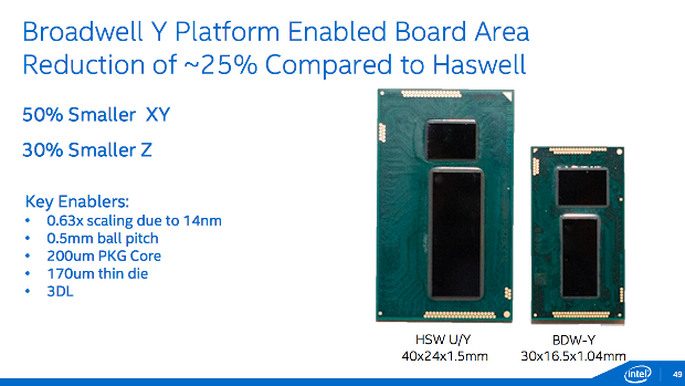
Broadwell-Y and Haswell-U/Y modules appear to have a platform hub controller die in common. Source: Intel.
Similarly Intel has not said how many processor cores are included in Broadwell but as Haswell for mobile applications had two or four cores, it is reasonable to suppose that Broadwell, which is essentially a shrink of Haswell, has at least two. Broadwell-Y as a dual-core processor was confirmed by the Intel spokesperson.
Intel was more forthcoming when it came to making claims about performance improvements over Haswell. Larger translation lookaside buffers and pages, a larger out-of-order scheduler and faster store-to-load forwarding result in a more than 5 percent improvement in instructions per clock cycle. Broadwell also includes instruction execution improvements targeted at cryptography acceleration, the company said.
In terms of graphics Intel was again less forthcoming about what Broadwell contains but was eager to talk about relative performance improvments. As Haswell-Y includes either GT2 or GT3 graphics processing units (GPUs) the first assumption is that Broadwell has the same but improved through the use of 14nm FinFET manufacturing process.
Intel claims that Broadwell graphics performs 20 percent more computations and has a 50 percent higher sampler throughput. Something call the Video Quality Engine has twice the throughput of Haswell and there is native support for 4K and Ultra High Definition video. In terms of software the GPUs now support Direct X 11.2, OpenGL 4.3, OpenCL 1.2 and 2.0, which are a series of standards and APIs for graphics rendering and GPU-computation.
More detail of the design of Broadwell and its companion in-package chip is expected to come at the Intel Developer Forum in San Francisco September 9 to 11, 2014.
Related links and articles:
News articles:
Intel Partners With Rockchip For Tablet Push
