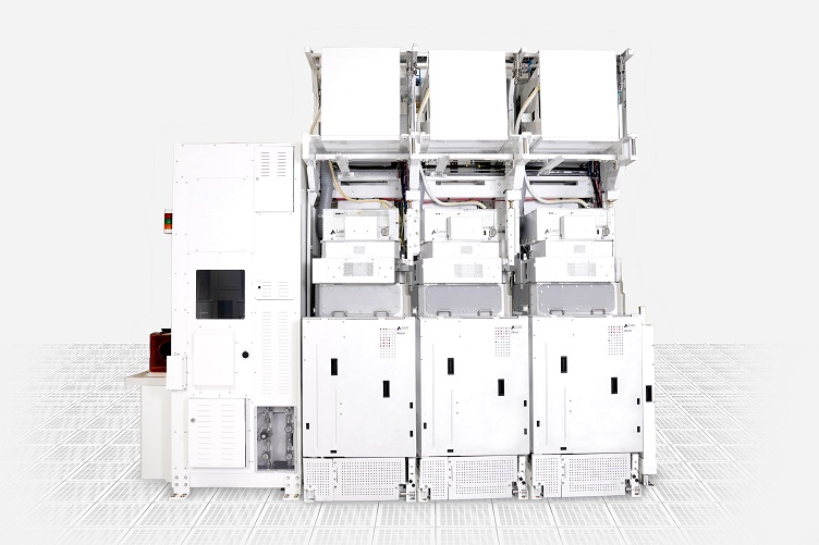
Lam Research Corp. has rolled out what it claims is an advanced plasma conductor etch tool needed for 3D chipmaking.
Called Akara, the device is the successor to Lam’s Kiyo conductor etch tool that was introduced in 2004 and has more than 30,000 chambers in production.
Akara enables the scaling of gate-all-around (GAA) transistors and 6F2 DRAM and 3D NAND devices. It is extendable for 4F2 DRAM, complementary field effect transistors and 3D DRAM. These devices require critical etch steps and precise extreme ultraviolent (EUV) lithography patterns to form complex 3D structures, Lam said.
"As global demand for semiconductors continues to grow, innovative technology solutions from our partners are required to enable new, more powerful device architectures," said Y.J. Mii, executive vice president and co-chief operating officer at TSMC. "Critical plasma etch capabilities will be an integral part of solving the many production challenges these new devices pose."
Three main features of the etch tool include:
- Solid-state plasma source
- Plasma species control
- Ion energy control system
DirectDrive is what Lam claims is the first in the industry to generate 100 times faster responsiveness than previous sources, resulting in fewer EUV patterning defects. The Tempo plasma pulsing provides microloading performance to control plasma species. Finally, SNAP is the energy control system that shapes the etch profile with atomic precision.
Additionally, Akara improves wafer output with millisecond response times and can ensure wafer-to-wafer repeatability.
