A new method for integrated circuit testing combines two common approaches into a single technology.
Vertical spring probes have traditionally been used to test some of the most common packaging schemes for integrated circuits, including ball grid array (BGA), land grid array (LGA), quad flat no-leads (QFN) and quad flat package (QFP). The method is not without its drawbacks, however, as the piercing effect of spring probes on the gold pads of a printed circuit board can cause a buildup of surface oxides. By contrast, the cantilever scrubbing contact design often used to test peripheral segments removes surface oxides and contaminants — yet it can cause expensive damage to the PCB.
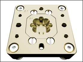 The Kepler test socket combines the scrub motion of a cantilever contact with the modular action of a spring probe. Source: Smiths InterconnectAs a result, both technologies require maintenance and performance monitoring to ensure optimal results during testing cycles.
To answer these challenges, connectivity solutions provider Smiths Interconnect has developed what it calls a breakthrough technology: the Kepler test socket. Kepler combines the scrub motion of a cantilever contact with the modular action of a spring probe. It includes horizontal movement during the downward stroke of the device to break surface oxides and provide stable and reliable contact without causing PCB damage.
According to the company, Kepler is the only testing solution that provides two axes of motion during a single actuation of the socket. Its benefits can be seen in a boosted first pass yield, enhanced production reliability and extended maintenance intervals.
Additional benefits include:
- Long contact life, low wear; tested to over 500,000 insertions
- Short signal path, exceptional signal integrity
- Small socket footprint
- Socket design supports temperature range from -55° C to 150° C
- Low dielectric constant, low coefficient of linear thermal expansion (CLTE), exceptional flexural modulus
- Reliable and consistent contact for matte tin or nickel-palladium-gold pads; low and consistent contact resistance (CRES)
- Configurable design flexibility for integration into existing hardware setups
- Allows for PCB topside components to be placed close to the device under test for better signal performance and less signal loss
- Field repairable; easy cleaning and maintenance
The Kepler test socket is designed for manual testing, bench testing or high-volume manufacturing (HVM) production testing.
