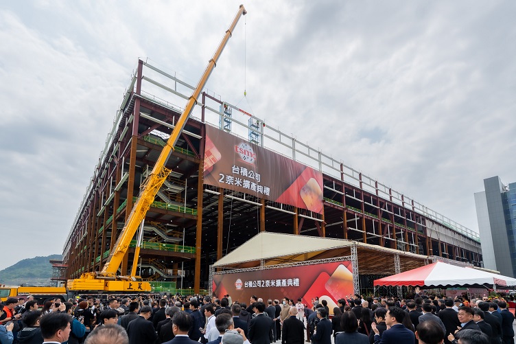
The world’s largest chipmaker and pure play foundry Taiwan Semiconductor Manufacturing Co. (TSMC) is expanding its 2 nm capacity at Fab 22 in Kaohsiung, Taiwan’s Southern Taiwan Science Park. But what does this mean for the overall global semiconductor manufacturing?
TSMC said that its 2 nm technology will enable a 10% to 15% increase in speed at the same amount of power consumption. It will also enable a 25% to 30% reduction in power at the same speed, compared to the previous generation process technology.
Additionally, the company said the 2 nm technology will enable its users to sell $2 trillion worth of semiconductors across all major markets in five years of volume production. This includes markets like automotive, smartphones, data centers, cloud computing, AI and supercomputers.
Why it matters
TSMC’s Fab 22 is likely to be the lead 2 nm production facility in the world until other fabs — like the four fabs being constructed in Arizona — come online.
The 2 nm tape-outs will outpace 3 nm in the first two years. Initial 2 nm volume production at Fab 22 is likely to begin in the second half of this year, according to a report from Reuters.
TSMC said it is potentially open to building a sixth fab at the location in Kaohsiung. Currently it has three fabs operational with two more under construction. In total, TSMC will build nine advanced fabs in Taiwan: five 2 nm fabs in Kaohsiung, one 2 nm fab in Hsinchu, three 1.4 nm fabs in Taichung and Hsinchu, and three advanced packaging plants in Chiayi and Tainan.
Further expansion
The new fabs in Taiwan are not the only moves TSMC is making. The company is also expanding in the U.S. after TSMC announced it would invest an additional $100 billion in U.S. semiconductor manufacturing at its Phoenix, Arizona, location where it has already invested $65 billion.
The expansion will include:
- Three new fabrication plants
- Two advanced packaging facilities
- One R&D team center
TSMC also broke ground in Germany, its first European fab, in August of 2024. The company plans to invest about $11 billion with the hope that it will garner direct funding from the European Chips Act.
Another two fabs are being constructed in Japan by TSMC.
The company is already the largest chipmaker in the world and these investments will likely set the company to new heights.
