On-chip optical isolators remain the elusive holy grail of integrated photonics. For coherent photonics, an optical isolator remains as vital as the laser device itself.
As photonics expands beyond its traditional telecoms footprint and into areas like biophotonics and sensing, the commercial prize of an integrated isolator is greater than ever. There are five main performance objectives for an integrated isolator.
- Easy integration (easily manufacturable)
- Small footprint
- Low material loss and back-scattering
- Necessary bandwidth
- Minimum required isolation (probably the most obvious)
For any kind of coherent photonics, the last two specifications are clear: 40 dB across the gain band of the laser device. For less refined photonics, these values can be relaxed somewhat. What follows is a look at the active versus passive methods, the required materials, the device level aspects and, finally, any workarounds for the problem.
Three approaches to solving this problem have been put forward. The first is time-dependent modulation; the second is the use of non-linear optical effects; and finally, a method based on the Faraday effect, or to a lesser extent birefringence of semiconductor materials.
The first two approaches will always struggle with simplicity and footprint issues as they are active methods. As so, they have been less favored in terms of ongoing research. The Faraday effect method is the most promising due to simplicity.
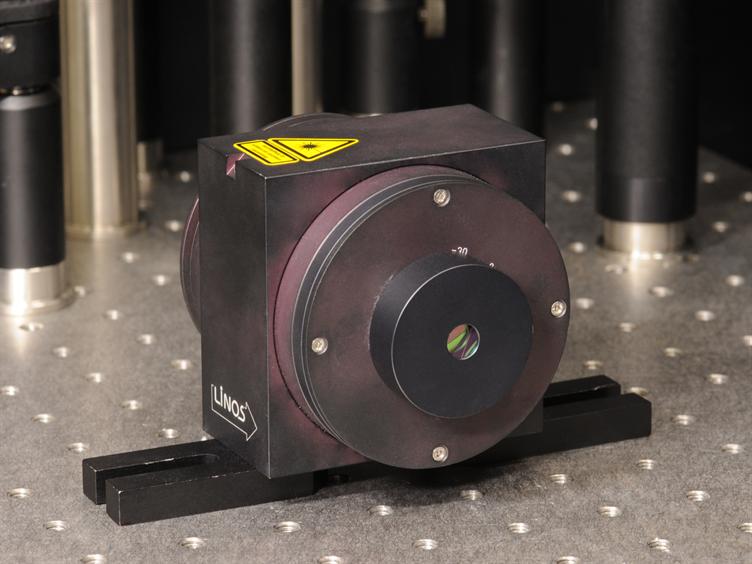
The Faraday effect is where a magneto-optic material interacts with the electric field component of light and rotates polarization when a magnetic field is applied. The effect is non-reciprocal, so reflected light can be easily filtered out using a polarizer. Birefringence is another physical principle that can be exploited here; this is where one polarization sees a different refractive index to its orthogonal mode due to the material structure. Birefringence is less common, as it tends to provide less polarization selectivity than Faraday rotation. Faraday rotators, if combined with other components such as polarizers, can achieve directional isolation. 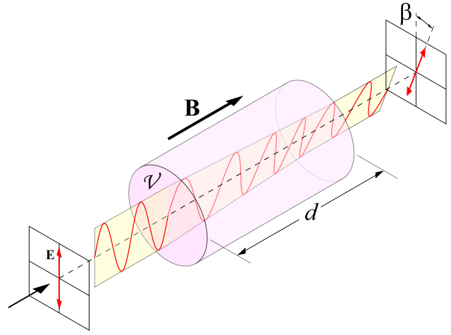 Faraday rotation. Source: DrBob/ CC BY SA 3.0
An integrated polarizer remains the main stumbling block with this development. Also, applying a magnetic material to create a magnetic field can be difficult. This type of isolation is polarization-dependent isolation.
Polarization-independent isolators are also possible with more complicated designs. Polarization-independent isolation is more desirable as when a device is in situ, polarization cannot be tuned, which could cause excessive loss and impact the yield on integrated devices. Mach-Zehnder Interferometers (MZIs) are the chief architecture of polarization-independent integrated isolators, but other structures such as ring isolators have also been considered. MZI solutions, however, suffer from a lack of bandwidth, given the basis on destructive phase interference, but at the moment also seem like the most promising method.
Integrated photonics is becoming increasingly silicon-based, meaning integrated isolators are being targeted for this platform also. Magneto-optic garnets are the near-standard material for Faraday rotators. Garnet can be grown or printed on silicon, and each method has its difficulties. Integration by growth was initially favored as it surmounted the high temperatures involved in bonding. Garnets are traditionally grown with liquid phase epitaxy, whereas semiconductors are grown by vapor phase epitaxy. Garnets also show quite different crystal dimensions to traditional semiconductor substrates. These aspects make controlled growth difficult, but easier than high-temperature bonding.
The significant difference in thermal expansion coefficients between garnets and traditional semiconductors induces cracking during high-temperature annealing in bonding. Performance requirements are high, making the growth very sensitive to defects and cracks along the device waveguide. Wafer bonding techniques are continuously improving. If transfer and bonding become the industry standard technique of integrated photonics production, so too would the efforts of developing bonded techniques of isolator integration, despite the benefits of garnet integration by growth.
Regardless of production difficulties, garnets are still not ideal materials for integrated optical engineering. Garnets are of low refractive index, reducing mode confinement and increasing loss as a waveguide. As much as the difficulties in the mismatch in growth are an issue, the mismatch in structure between the magneto-optic material and the traditional semiconductor input and output will cause back-scattering and loss by its nature. Garnets also have a significant material loss due to their low bandgap energy (i.e., cerium: yttrium-iron-garnet).
Doping of the waveguide is a simple alternative and can provide the necessary polarization rotation and maximum loss. Iron is particularly effective as a dopant here, as it is quite magnetically interactive but also low loss. The inherent difficulty with doping the waveguide is that the asymmetry of the waveguide means a controlled rotation between two polarizations is difficult, as both energy states are non-degenerate. Grown garnets can also be afflicted by these difficulties.
One final angle has to be examined in this quandary: removing the necessity for the optical isolator to begin with. Quantum dot lasers have recently shown remarkable tolerances to back reflections, but are less suitable when it comes to the footprint, as the material gain is quite low. A quantum dot laser will have a cavity in the region of three times longer than a quantum well laser. An external optical isolator could perhaps beat this footprint, and retain the more power-efficient quantum well device. However, particularly if an MZI method is chosen, an integrated optical isolator will require many more production steps and will make the device more complicated to produce.
Luckily, this is an area under quite promising research. While there is always a gap between what can happen in the lab and what can happen in the factory, current research is focused on manufacturable solutions. Integrated optical isolators appear to be the technology of the near future, as opposed to the far future. However, it will initially be limited bandwidth, complex structures.
