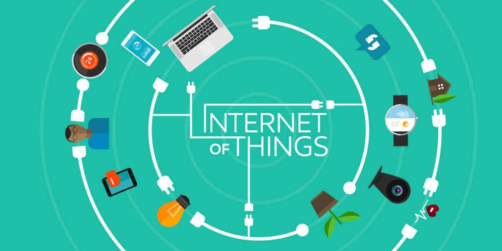
The internet of things (IoT) promises to change how we interact with the world. Sensors and cameras will capture exabytes of data, process it and then adjust heating, lighting, locks, alarms and countless other things in order to make our lives easier and our world more efficient. Analysts at Gartner project that there will be 20 billion internet-connected devices by 2020. These devices will include everything from vending machines, cars, to home sensors and environmental controls. Each of these devices will require integrated circuits (ICs) that contain embedded technology to communicate and sense or interact with the environment. The demands and constraints on these ICs are significantly going to alter IC design.
 The IoT will place new demands and constraints on IC design.IoT devices often include sensors, microelectromechanical systems (MEMS), controllers, processors, memory and Wi-Fi/Communication along with other analog and digital circuitry, all combined into space about a third of the size of a smartphone. The size constraints are significant and will pose substantial challenges for IC designers. Designs will likely require high density interconnect (HDI) boards. HDI boards allow designers to place more components on both sides of the printed circuit board (PCB) and closer together. Packages will also be more efficient, with multi-chip modules (MCM) and three-dimensional ICs (3D-ICs), allowing multiple circuits to be connected on a single die or in a stacked configuration.
This new, compact form factor will undoubtedly lead to electromagnetic interference (EMI) issues. In fact, in an IEEE IoT report, it was found that most new IoT devices fail EMI testing. Improved EMI software modeling is being developed to address these issues earlier in the design stage. For now, EMI testing is a critical aspect of the design process. Increasingly IC designers will have to carefully consider the impact of the location of the components with respect to each other on the IC as well as the IC itself in the packaging and the environment. It will not be enough to simply design a PCB and hand it off to another team for integration. All aspects of the product will have to be considered in the design process.
IoT devices, beyond size constraints, often have physical property constraints as well. Temperature, humidity and salinity resistance might be a requirement for a given application. Wear and flexibility may be considerations as well. Many of these devices will not be the traditional rigid ICs that have dominated the industry up until now. Certainly, as we move into the future more unconventional materials such as plastics and flex-rigid copper will be used. These new materials will have different design requirements. Additionally, power consumption is always going to be under pressure for IoT devices. These devices are generally battery powered and in order to be practical, shouldn’t require a battery swap more than a few times a year. Efficient power consumption will be a major requirement of all designs.
Finally, the IoT is mostly going to be composed of commodity devices. This means that while designing compact, power efficient, interference resistant ICs with evolving materials, it will have to be cheap and reliable as well. Swapping out components on a circuit board will be impractical under the conditions described above. in the design process, emphasis will be placed on simulation. Software will become increasingly important to save testing costs down the road. The process of design-test-redesign-retest is not going to be as forgiving as before. Getting it right in the first couple of design cycles will be essential.
The IoT is set to transform the way people interact with the world. The tremendous amount of data it captures will be used to introduce convenience and efficiency in our everyday lives. The demands on IC design will be significant, with ever-shrinking form factors, power consumption and costs. Designers will be forced to lean heavily on software early in the design process to improve reliability and reduce EMI issues. There will be a learning curve with respect to new materials and harsher real-world conditions. The challenges are significant going forward, but this has always been the case when technology takes a leap forward. What is certain is a decade from now the form factors used today will dwarf the small compact smart devices of tomorrow.
