Leti, a research institute at CEA Tech, and CMP, a service organization that provides prototyping and low-volume production of ICs and MEMS, announces the integrated-circuit industry’s first multi-project-wafer (MPW) process for fabricating, emerging, non-volatile memory, OxRAM devices on a 200 mm foundry base-wafer platform.
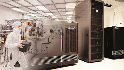
 Source: LetiAvailable on Leti’s 200 mm CMOS line, the MPW service provides a comprehensive, low-cost way to explore techniques designed to achieve miniaturized, high-density components. Including Leti’s Memory Advanced Demonstrator (MAD) future mask set with disruptive OxRAM (oxide-based resistive RAM) technology, Leti’s integrated silicon memory platform is developed for backend memories and non-volatility associated with embedded designs. The new technology platform will be based on titanium-doped hafnium oxide (HfO2/Ti) active layers.
Emerging OxRAM non-volatile memory is one of the promising technologies to be implemented for classical embedded memory applications on advanced nodes like micro-controllers or secure products, as well as for AI accelerators and neuromorphic computing.
Leti’s MAD platform is dedicated to advanced non-volatile memories, bringing both versatility and robustness for material and interface assessment, and allowing in-depth exploration of memory performance from technology and design perspectives.
The full platform’s highlights:
• 200 mm STMicroelectronics HCMOS9A base wafers in 130nm node
• All routing is made on ST base wafers from M1 to M4 (included)
• Leti’s OxRAM memory module is fabricated on top
• One level of interconnect (i.e., M5) plus pads are fabricated in Leti’s cleanroom.
The MPW service with integrated silicon OxRAM addresses all the key steps of advanced memory development. These include material engineering and analysis, developing critical memory modules, evaluation of memory cells coupled with electrical tests, modeling and innovative design techniques to comply with circuit design opportunities and constraints. This technology offer comes with a design kit, including layout, verification and simulation capabilities. Libraries are provided with a comprehensive list of active and passive electro-optical components. The design kit environment is compatible with all offers through CMP.
Providing access to a non-volatile memory process from Leti is a major achievement in development work at CMP. Since 2003, the organization has participated in national and European projects for developing access to NVM technologies (Mag-SPICE, Calomag, Cilomag, Spin and Dipmem). With this new offer in place, the CMP users’ community can have the benefits and advantages of using this process through this close collaboration between CMP and Leti.
“CMP has a long experience providing smaller organizations with access to advanced manufacturing technologies, and there is very strong interest in the CMP community in designing and prototyping ICs using this process,” said Jean-Christophe Crébier, director of CMP. “It is an opportunity for many universities, start-ups and SMEs in France, Europe, North America and Asia to take advantage of this new technology and MPW service.”

