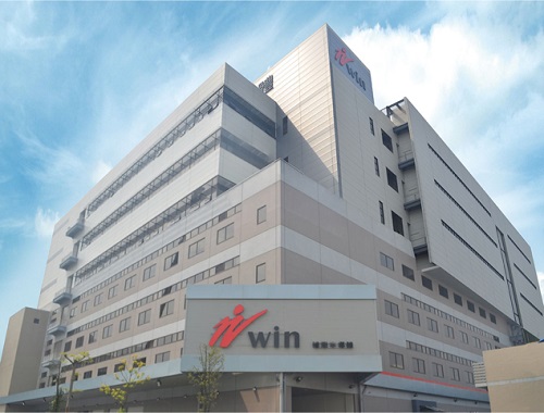
 Win’s Fab C facility is located in Guishan, Toayuan City, Taiwan. Image credit: Win Semiconductors
WIN Semiconductors Corp. has completed the second phase of its expansion to its Fab C semiconductor facility.
Fab C now has been fitted with clean rooms, process lines and equipment for gallium arsenide (GaAs) MMIC production, epitaxial growth of compound semiconductors as well as fabrication and test of optical devices.
The pure-play GaN and GaAs foundry says the expansion will support WIN’s portfolio of hetero-junction bipolar transistor (HBT), pseudomorphic high electron mobility transistor (pHEMT), integrated BiHEMT technology and optical technology for use in mobile PA, WiFi, wireless infrastructure and optical markets.
WIN says the foundry manufacturing services support most applications from 50MHz to 150GHz and through light-wave.
The wafer Fab C facility is located in Guishan, Toayuan City, Taiwan, and when fully built out will more than double the company’s capacity, WIN says.
