PCB designers usually treat metrology as a manufacturing or quality problem that starts after release. That view is now becoming outdated given that more designs deal with fine features and package interfaces pushing into very high bandwidths. If the fabricator or lab cannot measure the structure with enough fidelity and repeatability, then qualification, process control and model correlation all become uncertain. NIST’s CHIPS Metrology Program makes the broader point clearly: measurements need to be accurate, precise and fit for purpose if you want microelectronic production to scale.
Advanced packaging suppliers have already organized around that idea because smaller features and heterogeneous integration demand tighter process control and traceability, but the PCB industry has not moved at the same pace. As a result, new levels of automation are needed in metrology for packages and PCB, and as a result the metrology practices in both areas will start to look very similar.
PCB metrology struggles to keep up with demand
Industry metrology standards have continued to scale their applicability to smaller feature sizes, but that does not mean QC teams and labs are able to keep up with demand. In reality, the smaller feature size scales, one would expect greater demand given the reliability challenges present at smaller feature sizes.
In terms of standards, IPC still places microsectioning squarely inside the compliance and qualification framework. For example:
- IPC-TM-650 defines microsections as the basis for evaluating laminate systems and plated structures
- IPC-6012 explicitly includes structural integrity requirements for microsectioned coupons or printed boards, along with qualification test coupons and coupon selection
- IPC-2221 (Appendix A) defines design requirements for test coupons, including coupons for microsection analysis (e.g., A/R, D, S)
While this is all helpful for standardizing qualification, these standards were developed at times when most of the lab metrology work and subsequent analysis were performed manually. Some automation has come to the space in the form of data analysis and collaboration features. But the actual execution of measurements still relies heavily on the skill of equipment operators. Coss-sectioning is highly manual, highly dependent on operator skill, and subject to stochastic variation, especially when attempting to hit the correct plane through very small structures.
“We found it on both the manufacturer and the OEM side, that it’s highly manual,” said Geoffrey Leads, founder of ScanLabs. “It’s very operator dependent. There’s a lot of stochastic variation in that process. And some operators do things a little differently from each other, so it’s really kind of the Wild West.”
Currently, standards only tell a lab or QC team what must be evaluated, but it does nothing to help generate consistent, high-throughput data that can be fed back to process engineering or the product designers. IPC has a defined semi-automatic microsectioning method, but even that method still depends on multiple steps preparation quality, planar grinding, polishing setup, etching and evaluation against the customer specification. In many ways, this presents an opportunity for automating metrology systems to provide higher throughput and more frequent testing.
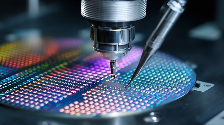
 Metrology electronics manufacturing is struggling to keep up with demand. Source: Sardar/Adobe Stock
Can we use an alternative to AOI and microsections?
The answer is: probably not…
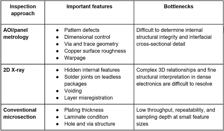
One might suggest switching to a measurement technique that already enjoys automation, such as X-ray scanning. While extremely useful, 2D radiographic methods have significant limitations on increasingly complex electronics, which is why 3D imaging methods are being pushed harder in semiconductor inspection. In PCBs, X-ray can show a lot, but it does not automatically give you the structural cross-sectional fidelity you need for plating integrity, crack initiation, interfacial geometry or microvia assessment that is demanded in high-reliability industries.
AOI, panel metrology, X-ray and destructive cross-section each see different portions of a PCB with different degrees of automation and accuracy. In PCB quality control, these methods are all single-frame, and in the case of an inexperienced operator, you might only get an accurate frame by chance. Furthermore, these processes are limited by the speed at which a human can perform the necessary task, and that is precisely where the critical shortage of skilled operators becomes obvious.
This lack of throughput has created a hidden backlog problem, where some OEMs and contract manufacturers have so many metrology samples that require analysis, yet their staff of skilled operators can’t keep up with the demand. This is especially problematic in high-reliability industries (e.g., aerospace) where large numbers of PCB samples are needed to prove that bare PCBs or assemblies are reliable. That operator dependence is one of the clearest points of opportunity for metrology automation.
Borrowing process-control flow
PCB metrology should learn from semiconductor and package metrology, not because the materials are identical, but because the measurement problem is already familiar there. Advanced packaging has lived with small features, traceability, yield excursions and tight process windows for years. PCB fabrication is now running into the same class of problem at larger scale and different cost structure.
A useful version of that approach is already visible in the market: keep a standard coupon but automate the data extraction around it. A method built around serialized grinding, repeated imaging and spatial correlation of defects allows a coupon to be reconstructed as a richer data object rather than a single pass-fail image.
“So in our piece of equipment, we actually know ahead of time … if there is a theoretical perfect cross sectional plane that’ll hit everything,” Leads said. “If not, we can serially step through it. So we’ll grind to the very first plane, take a micrograph, and then grind down a bit more to the next plane, take a micrograph, and so on.”
This approach matters because a single micrograph may show whether one cut location is acceptable, while a sequence of aligned sections can reveal rotation, tilt, registration behavior, glass-resin interaction and volumetric geometry in ways a one-plane slice cannot.
That is where PCB metrology starts becoming more useful to designers. Once you can reconstruct a structure in 3D or at least correlate multiple sections spatially, you can feed as-built geometry back into electrical, thermal and mechanical models. Given today’s automated image capture and reconstruction capabilities, it is possible to reconstruct digital geometry from coupon analysis for reuse in simulation. That is a much better direction than leaving coupon data trapped in static PDF reports that only serve a compliance audit.
