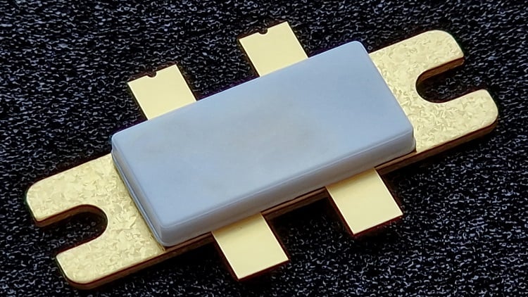
GaN-based and SiC-based power system designs are being implemented for their high-power handling and efficiency at higher voltages, currents and frequencies, despite the higher costs. These systems extend performance range for power designs in common topologies and form factors, and with efficiency that has the ability to reduce the thermal load on a system operating at a given power. It makes sense that some applications are expected to see GaN become the dominant materials platform for FETs, such as GaN-on-Si in RF power amplifiers.
Although the performance and efficiency gains seen with these components are noteworthy, higher efficiency does not preclude system-level and PCB-level design practices that can help manage heat generation during operation. Component-specific performance gains can quickly be lost if the physical layout and enclosure design cannot accommodate the thermal load generated in these systems. As such, I’ll discuss some little-known best practices for enclosure design and PCB design in this article.
How to manage heat in GaN/SiC-based systems
Because GaN and SiC devices support much higher switching speeds and power densities than silicon, the thermal burden in a system can scale rapidly if heat isn’t transported away from these components. Although wide-bandgap devices can reduce switching losses, the residual dissipation becomes concentrated in small junction areas. Without careful thermal design, local temperature rise will degrade performance (mobility, threshold shift) and ultimately threaten device reliability, negating many of the advantages of GaN/SiC in the first place.
The first place to start with system-level design is with a good PCB layout, which includes elements such as:
- Large copper pours
- Heavier copper layers (up to 2 to 3 oz/sq ft)
- Thermal vias under die-attached pads
- Higher plane layer counts at high current
These are fundamental PCB design practices that apply in a range of products. However, their overgenerality means there is more to be done to ensure high-power GaN/SiC-based power electronics are reliable and thermally efficient.
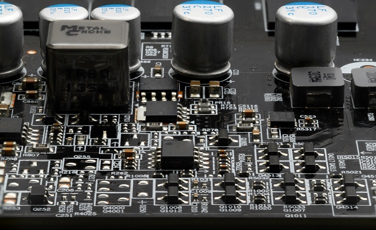
FET arrangement on the PCB
It is well-known that placement of parts and routing on a PCB have a major impact on noise, EMI and signal integrity. PCB layout also impacts the reliability of FETs in power systems, which still predominantly use large arrays of FETs. While physically large individual GaN/SiC FETs are available and used in applications like inverters for EVs, many other power systems will continue to use arrays of smaller, faster GaN/SiC FETs, which are arranged in parallel.
Enforcing symmetry in the arrangement of FETs can prevent device failure due to symmetric flow of current (and thus power dissipation) across the FET array.
“The symmetry of the arrangement is super important,” said Caleb Buck, Electronics Engineer at Nidec Aerospace. “If you’re sourcing multiple FETs in parallel, you need to attempt to allow current to flow symmetrically to the FETs with respect to each other, otherwise you can have your load poorly distributed across your devices. This can lead to overheating on certain devices, even though a device array should theoretically be able to handle the electrical load."
Such an arrangement would look like that shown below.
 An example of a FET array. Source: John/Adobe Stock
Enclosure as a heat sink
Electronic enclosures tend to have high thermal mass, which gives an opportunity to use them as a heat sink for a design. By building a heat sink into the enclosure, or by bonding components directly into an element of the enclosure, the enclosure can serve as a heat sink for hot components.
In power systems, which will use GaN or SiC FETs, we can expect many system deployments to be placed in IP-rated enclosures, which eliminates the use of fans for cooling components. Using the enclosure as a heat sink, particularly a metalized enclosure, gives desirable thermal conductivity and high thermal mass needed to dissipate a large amount of heat from hot components. One should note that higher power densities (i.e., small enclosures) may result in highly localized heat, and enclosure touch temperature could be too high. Make sure to account for this during design, simulation and testing of your system.
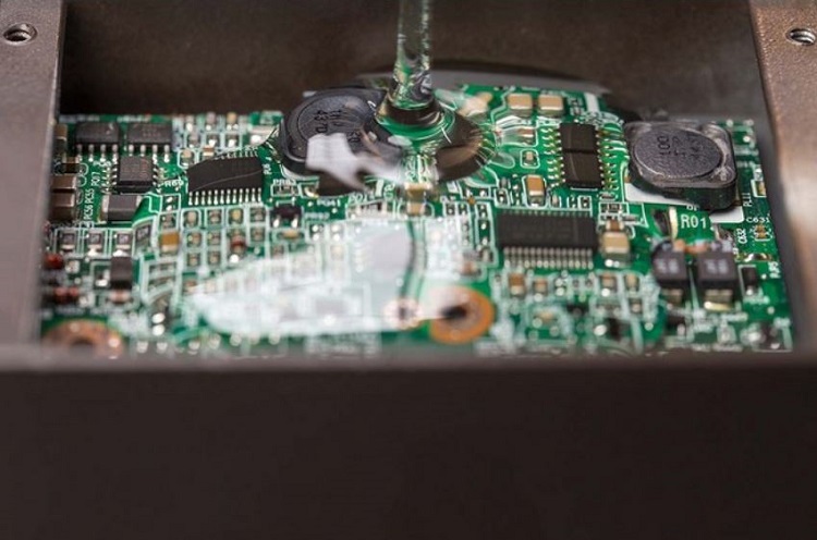
Thermal interface materials and thermal potting
There are additional materials that can be used in an assembly to increase heat dissipation from hot components. One option is to use encapsulation, which works well in systems that do not have outgassing requirements. Caleb Buck provides more guidance on the use of encapsulants:
“Some of the other things you can do to help with heat are non-layout heat spreading techniques, such as thermal potting, that…essentially encapsulate your hot parts through a thermally conductive material,” Buck said. “This gets the heat out away, not through the board, but through the thermally conductive potting.”
Thermal potting refers specifically to highly thermally conductive potting materials, which can very efficiently conduct heat to an enclosure. Many thermally conductive potting materials are also absorbers of electromagnetic waves at MHz and GHz frequencies. For GaN FET arrays, which can be switched at much higher frequencies than silicon FETs, these potting materials serve an additional purpose of emissions control, particularly when driving high currents through the system's switching node.
 A variety of thermally conductive materials can be used for potting and heat management. Source: XYJ Silicones
Another common option for increasing the spread of heat away from hot components is to use a thermal interface material on heat sinks and any surface-to-surface bonds to enclosures. These materials are also adhesive materials that will increase the mechanical strength of heat sinks bonded onto hot components.
Thermal potting and TIMs are both excellent ways to provide a low thermal resistance interface between a hot group of components and an enclosure or heat sink. The TIMs and thermal potting materials have high thermal conductivity and are shape-conforming materials,
Conclusion
Electrification and upgrading energy infrastructure are long-term trends where GaN, SiC and stacks of these materials will see greater use in a wide range of applications. From electric vehicles to renewables management, these materials can make power systems more efficient both electrically and thermally as long as well-understood system-level designs considerations are implemented.
This means a renewed focus on thermal management practices in PCB and packaging design is needed. If implemented correctly at the board level and enclosure level, power systems can continue to extend the performance envelope to higher power outputs and frequencies.
