Metals and dielectrics are the building blocks of metamaterials, which are artificial materials that span all three dimensions. To achieve the desired bulk behavior, engineers generally arrange a number of tiny scatterers (such as spherical magneto-dielectric particles or metallic rings and rods) in a continuous sequence across a certain volume of space. To further develop this idea, electrically tiny scatterers can be strategically arranged in a 2D pattern at a surface or interface. Planar, 2D, subwavelength-thick variants of metamaterials are known as metasurfaces. Their simplicity of construction and light weight have made them a prime candidate for use in electromagnetics.
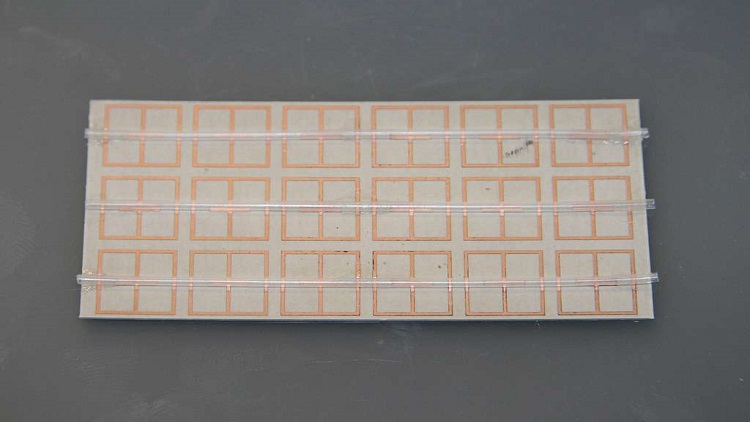
Structure and functionality of a metasurface
Metasurfaces are planar structures that make use of the interactions between light and engineered subwavelength elements. Meta-atoms, as these elements are sometimes called, can be engineered to have certain optical characteristics. The two fundamental types of metasurfaces are dielectric and plasmonic metasurfaces. Dielectric metasurfaces manipulate light using the refractive index contrast between different materials, while plasmonic metasurfaces leverage the resonant oscillations of electrons on metal surfaces.
The functionality of metasurfaces arises from their ability to control the phase of incident light. By strategically arranging meta-atoms, metasurfaces can impose a specific phase shift on incoming light waves, leading to various optical phenomena such as lensing, holography and beam steering. The control over the amplitude and polarization of light further expands the possibilities for customizing optical responses.
Applications of metasurfaces
- Precise scattering management: From microwave to optical frequencies, metasurfaces can block, absorb, concentrate, disperse or guide waves on the surface at grazing incidence as well as in space at normal and oblique incidence. Metasurface unit cells can be designed with the appropriate impedance to adjust the phase or group velocity of surface waves. They are employed in applications that need precise management of scattering, as their patterns direct or divide waves in certain directions.
- For surface waveguides: Metasurfaces may be used to adjust the phase or group velocity of surface waves by creating metasurface unit cells with the appropriate impedance. They are utilized in scattering control applications due to their patterning, which directs or splits waves in predetermined directions. Diverse effective surface refractive indices may be obtained, and the surface can be designed to serve different functionalities by adjusting the sizes and shapes of the metasurface unit cells. Surface waveguides are utilized for antenna systems and planar microwave sources, and they may be put to use in the creation of 2D microwave/optical lenses like fish-eye lenses and Luneburg.
- To control plane waves: Metasurfaces are also used to control plane waves in free space, in addition to surface waves. For uses as ultra-thin polarization transformers, the reflection phase of waves striking the metasurface may be adjusted. Incoming waves with linear polarization can be converted to waves with circular polarization by rotating them through 90°. Metasurfaces are also studied in depth as a potential tool for wavefront engineering, which includes beam shaping by means of defocusing, focusing, refraction and reflection. Coating curved and planar surfaces with metasurfaces reduces scattering, which is useful for cloaking and other applications in microwave and far-infrared frequency ranges. Metasurface absorbers can also be paired with active circuits or nonlinear devices as they have proved to be better than traditional absorbers.
- To emit waves: In addition to controlling the absorption and scattering of electromagnetic waves, metasurfaces may be used to emit waves into empty space in the form of a leaky wave antenna by converting surface waves to radiation modes, allowing precise manipulation of the radiation field. Traditional electronic components like lenses and waveguides can be bulky and limit the miniaturization of devices. Metasurfaces, with their ability to manipulate light at the nanoscale, offer a pathway to design compact and lightweight components. This is especially valuable in the development of miniaturized sensors, imaging devices and communication modules.
- For invisible cloak: A cloak is a device that can hide an item from incoming waves. Cloaking devices may be created with the use of metamaterials and transformation optics. Effectively creating ultrathin, low-loss, cloaks of arbitrary shape in three dimensions is possible by metasurfaces.
Trending developments
Other than huge planar wafers, the metasurfaces need to function on a wide variety of surfaces to meet a wide range of practical needs and work in tandem with a variety of devices. As a result, creating a soft metasurface that can bend or flex is one of the hottest new areas of research. Typically, a metal or metal-dielectric structure or purely dielectric materials are placed on a flexible substrate to create a soft metasurface. Meta-structures have been produced recently over 2D materials, carbon nanofilms and flexible polymers.
Conclusion
Metasurfaces have gained a great deal of interest due to their ability to execute wavefront modulation at the sub-wavelength scale. The 2D metasurfaces, composed of carefully crafted subwavelength elements, are rewriting the rules of manipulating electromagnetic waves. From shaping light beams to crafting ultrathin lenses and enabling futuristic communication devices, metasurfaces are captivating researchers and engineers alike with their potential to transform industries.
