Sponsored Content
MEMS and Sensors
Time domain simulation of electrostatic discharge testing
10 September 2019
Sponsored content
An electrostatic discharge (ESD) is the sudden flow of current between two electrically charged objects caused by the breakdown of the dielectrics separating them (i.e., dielectric breakdown). In the case of electronic devices, the resulting current flow and possible spark can permanently damage the device. An unsubstantiated quote often recited is, “Losses associated with ESD in the electronics industry are estimated at between a half billion and five billion dollars annually.”
In reality, it is extremely difficult to estimate the exact cost of ESD loss, but it can safely be stated that ESD requires the development and testing of many hardware prototypes in the design and manufacturing stages and contributes to a high number of warranty claims and loss of consumer confidence if failure occurs in the hands of the consumer. Therefore, electronics manufacturers go to great lengths to properly shield sensitive components and to design systems capable of reducing, dissipating and neutralizing static charge.
To test the ESD susceptibility of electronic devices, hardware engineers typically use a number of test models defined by standards from organizations including, but not limited to, the American National Standards Institute (ANSI), JEDEC and the International Electrotechnical Commission (IEC). These tests are generally performed using ESD simulators, or ESD guns, to apply high speed, high voltage pulses to various points of the device under test (DUT).
Even for an experienced engineer it can be extremely challenging to pinpoint the location of an ESD failure during testing, and in some cases, to determine if a failure occurred at all. ESD failures are typically categorized into three groups: catastrophic, latent or upset. In the case of a catastrophic failure, the DUT will no longer function and there is usually a sign of physical damage, such as melted or charred components. While intuitively catastrophic failure may sound like the worst-case scenario, it is in fact the most ideal for an ESD engineer to encounter during quality assurance testing because it can be easily recognized, located and accounted for in the final ESD mitigation design.
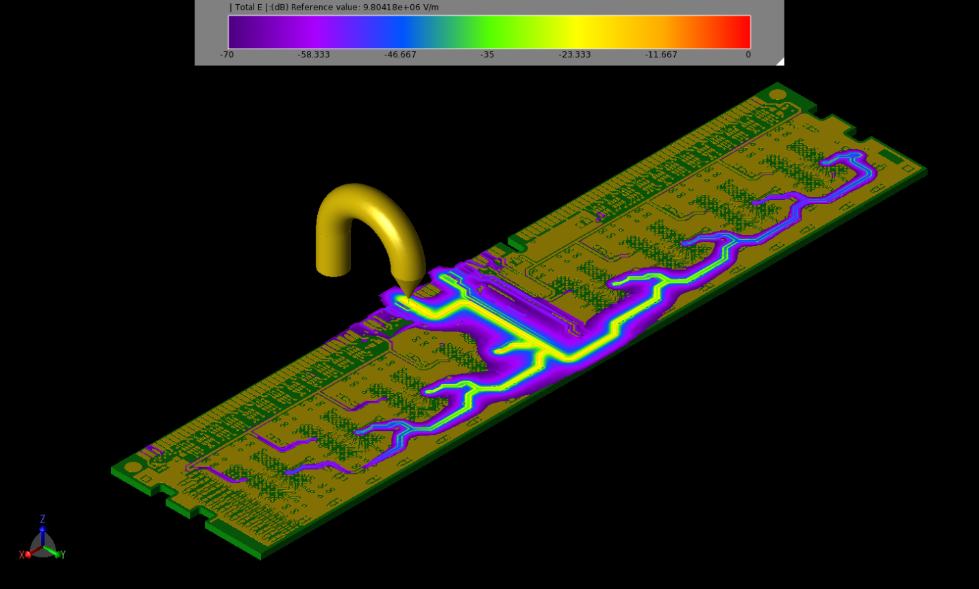 Figure 1: Electric fields during an ESD test of a DDR3 RAM stick. Source: Remcom
On the other hand, latent and upset failures can be much more difficult to diagnose because the DUT still functions and there is little or no sign of physical damage. Latent failures are often not visible with the naked eye and result in a weakened device that functions at the time of testing, but deteriorates over time with continued usage and will often malfunction or fail in the consumer’s possession. Upset failures are the result of over-currents that do not physically damage the DUT, but compromise components’ semiconductive properties leading to unpredictable behavior and data loss when used. Latent failures can sometimes be identified under magnification, but upset failures are nearly impossible to detect during testing.
Given the high cost in time and materials associated with ESD hardware testing and the difficulty of locating latent and upset failures, the ability to simulate the ESD testing process to pinpoint locations susceptible to ESD damage and optimize ESD mitigation during the concept and design stage of product development would be extremely valuable. In response to this growing need, a number of new ESD simulation features have recently been added to Remcom’s full wave electromagnetic simulation software package, XFdtd®. Using XFdtd’s improved user defined waveform feature, engineers can import ESD waveforms defined by the various testing standards and use them to create ESD current sources in their XFdtd project.
At this point, ESD simulator/gun models can be created and used to excite the DUT geometry at locations of interest and the resulting electromagnetic fields and current flows can be simulated and analyzed (Figure 1). However, the question of how to determine if and where an actual ESD failure occurred still persists. To solve this, a new material parameter, dielectric strength, was added to XFdtd’s electric material definitions. The dielectric strength of a material defines the maximum electric field it can withstand without experiencing dielectric breakdown (i.e., losing its insulating properties).
Upon adding the dielectric strength parameter to XFdtd, it is possible to monitor FDTD cell edges for potential dielectric breakdown during transient simulations using a dielectric breakdown near field sensor. This sensor instructs the XFdtd calculation engine to monitor cell edges for electric fields exceeding the dielectric strength of their constituent material and record instances at which dielectric breakdown is likely to occur. The sensor requires the user to define the free space dielectric strength that will be used for all edges that do not contain a defined material.
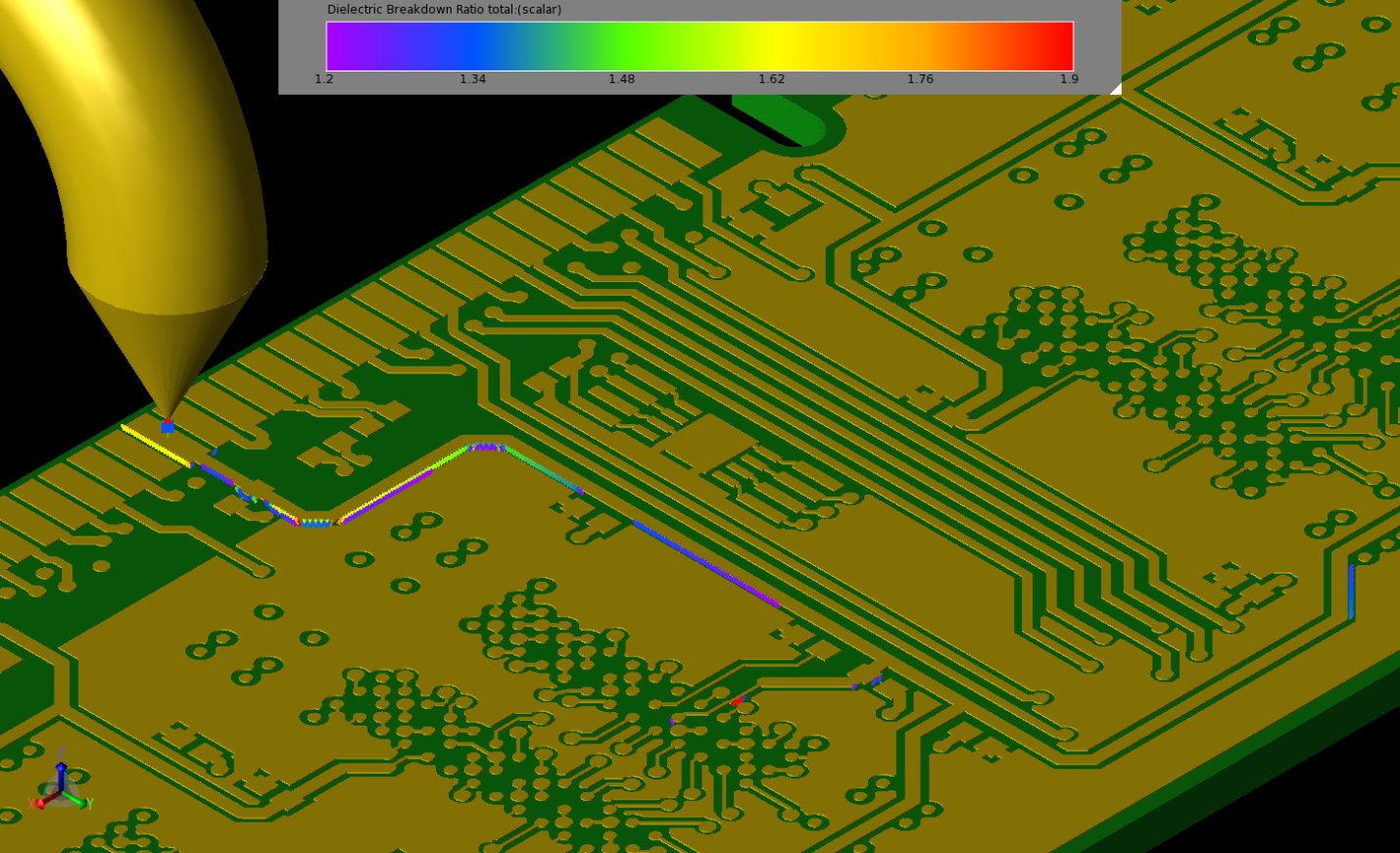 Figure 2: Locations predicted to be at risk of suffering dielectric breakdown during ESD testing. Source: Remcom
The default free space dielectric strength value is set to 3.0 MV/m, which corresponds to the dielectric strength of air at sea level. The sensor also allows the user to define a bounding box in order to limit the volume that is monitored for dielectric breakdown. The user can therefore obtain computational savings by defining specific areas of interest as opposed to examining the entire computational domain.
At the conclusion of a finite difference time domain (FDTD) simulation, cell edges that exceeded their dielectric strength can be viewed as shown in Figure 2. Additionally, functionality was added to XFdtd to monitor for electronic component failures during ESD testing. Rated voltage and current input parameters, which can be obtained from electronic component data sheets, were added to all of XFdtd’s circuit component types. This allows components that exceed their rated design parameters during ESD testing, which are subject to permanent damage, to be reported.
While simulation cannot and should not entirely replace hardware testing, these new computational features provide ESD engineers with more insight into probable locations of ESD failure and will allow ESD mitigation designs to be optimized prior to the hardware prototyping stage. Remcom believes this will reduce product development costs and time to market, while improving product reliability and consumer confidence.
Powered by CR4, the Engineering Community
Discussion – 0 comments
By posting a comment you confirm that you have read and accept our Posting Rules and Terms of Use.
Advertisement
Advertisement
Popular News
Find Free Electronics Datasheets

Advertisement