The current systems on chips (SoCs) are growing more complex. A smart phone alone may have between 20-25 processor cores enabling a variety of functions, Android or iOS, applications such as video and a myriad of app-store gems running on top. When developing such systems, it is a feat to find out if everything is working along the way, locating what is not, and speeding the process in order to stay competitive.
Ever since FPGAs made their way into the market in 1980s, they rapidly became a natural and important part of building and testing system prototypes of ASICs and SoCs. They also gave software developers early access to a functioning hardware platform. In short order, designs grew in complexity and size and FPGAs mirrored that growth with increased gate count.
Since an FPGA-based prototype provided a viable hardware platform long before silicon was available, early software tasks including OS integration and application testing moved up in the development cycle.
The Challenge
The downside of FPGA-based prototyping became visible as system complexity grew. Since many designs would not squeeze onto a single FPGA, they were partitioned across multiple devices. Not only did it take time, it was difficult for designers to reliably and efficiently work with several devices, interconnects could outnumber I/O pins and the PCBs required multiple layers, verifying became a nightmare, and mapping a design to FPGA prototype hardware was error prone and time consuming—with the process taking months.
Debugging using internal logic analyzers was also problematic since, while they addressed visibility, they had such limitations as support for a single FPGA debug, limited memory size and extended place-and-route times. Issues such as signal routing, capacitive loading and impedance matching limited prototyping, as well. Partition strategy, pin multiplexing, clock conversions and FPGA timing constraints also caused performance hits. As SoC multiplies in size, it may not translate well to older FPGAs.
Enter multicore SoCs and the levels of complexity and software content demands meant that systems engineers and software developers could no longer wait for hardware to jump in, so they increasingly needed prototypes of their chips and systems.
In the past, the approach was to make sure that the hardware was correct before taping out the chip. They simulated hardware using simulation technology, emulated hardware using emulators to fund the hardware bugs. In time they managed to get the hardware right, put the chip on a board and handed it to a software engineer who worked their magic and got the device out-the-door.
However, this process no longer works. The series of events is way too long for the fast-moving market where cycles have moved from 24 to 12 months, and it is not possible to create a secure chip. Software development would need to be done before the chip comes back from production.
In order to do software development before production, there must be a software representation of the chip. You cannot use a simulation, it is way too slow, and you cannot use emulation because it is still too slow for software development. It was necessary to find a way to prototype fast enough to do software and hardware development concurrently.
A study performed by Synopsys indicates that there are specific and consistent pain points that physical prototyping must address. These include:
- Mapping to FPGAs
- Debug Visibility
- Performance
- Capacity Issues
- Turnaround Time
Unfortunately, the existing prototype model could not keep up with any of these areas. The majority of prototyping is performed using disjointed tools and hardware. As the prototyping of small blocks gave way to prototyping sub-systems and full SoCs, at minimum, tools would be necessary to manage the complexity, and in reality, it would take more than just tools.
A Look at History
In Figure 1 below, prototyping tools are shown at the top and prototyping hardware at the bottom divided by a ragged line. This accurately shows the reality of the market. Designers often use prototyping hardware in house, then buy and use available tools in the market for prototyping and where they meet is, well ragged.
The use of generic tools is, for the most part, ineffective. The most important reason is that it is hard to tell when the prototype is working. In addition, companies that provide generic prototyping tools are in the dark as to exactly what type of hardware that will be used. What they offer may or may not be optimized for that hardware, and if not, the design is compromised.
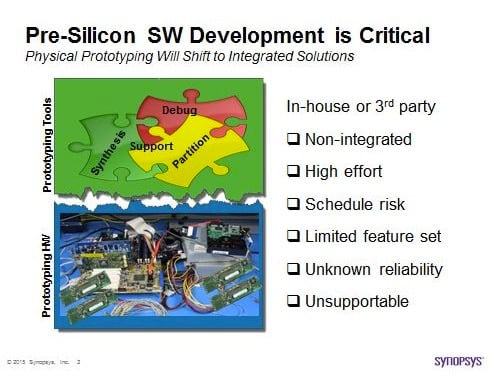
Figure 1. An indication of what is normal—generic prototyping tools and prototyping hardware, and the resulting challenges. Source: Synopsys
Finally, when a designer uses disparate tool and hardware providers, who will be motivated to step in and assist when there is a problem? Unfortunately, finger pointing starts rapidly in these situations. The reality is that this is the way the industry grew—but given today’s complexity, size, and need for speed—it just no longer works.
Which Brings Us to Today
Just as highly integrated SoCs became the norm, so to is high integration becoming the mantra of the prototype arena.
Only complete integration can drive the above-mentioned pain points to an acceptable level. An integrated prototype solution, as seen by a recent unveiling of the HAP-80 system by Synopsys, takes prototype time from months to two weeks on average; combined with the capacity of up to 1.6 billion ASIC gates, almost double the previous capabilities.
The Synopsys hybrid approach allows developers to freely mix pre-RTL transaction-level models with RTL that already exists, gaining a significant head start on hardware and software development. The solution combines virtual prototyping and FPGA-based prototyping to accelerate the development of SoC prototypes.
The Virtualizer virtual prototyping capability for new design functions and HAPS FPGA-based prototyping for reused logic and new RTL gives designers the ability to software development for up to 12 months earlier in the design cycle. The solution also enables designers to accelerate hardware/software integration and a full-system validation, reducing the overall product design cycle.
The ProtoCompiler portion of the Synopsys hybrid solution automates design flow and partitioning to reduce time to first prototype on average to less than two weeks and subsequent iterations to hours. The tool allows for the management of prototype board resources, enabling debug, partition logic and synthesis. Built-in debug capabilities are automatically inserted for greater debug efficiency and visibility, enabling the capture of thousands of RTL signals/FPGA.
What Next?
Today, with an integrated approach, months to prototype, have given way to a mere couple of weeks with our integrated approach. Somewhere in the future, the time will most likely shrink to two days.
The pain points mentioned above would not go away—they will continue to evolve and push the envelope for solutions. The process will likely be never ending.
