Fabless chip company Kalray SA (Orsay, France) is considering designing variants of its 256-core processor using the fully-depleted silicon-on-insulator (FDSOI) manufacturing process offered by STMicroelectronics NV. The company is also looking to scale back its 256-core processor to 64 cores to better address applications in areas such as automotive driver assistance systems and medical electronics.
A smaller version of its current MPPA-256 product is likely to be developed before Kalray moves up in performance with a 1024-core processor, according to Laurent Julliard, director of solutions and software services. He added that the FDSOI process is being considered for developments because of the power efficiency benefits it promises.
Kalray has been demonstrating a board with four MPPA-256 chips performing 4K-resolution HEVC encoding. This software-programmable solution has no video specific IP or ASICs and performs the encoding in less than 30-watts.
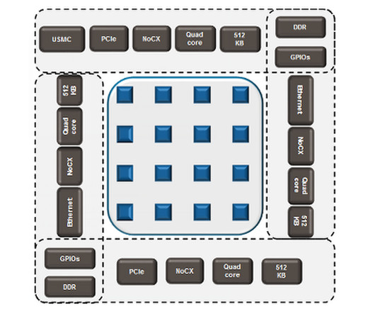
Block diagram of the MPPA-256 from Kalray which contains 16 clusters of 16 32bit VLIW cores.
The MPPA-256 is implemented in 28nm bulk CMOS and is manufactured for Kalray by foundry Taiwan Semiconductor Manufacturing Co. Ltd. (Hsinchu, Taiwan).
"Some customers have actually expressed their interest in an FDSOI-based implementation of the MPPA Manycore architecture," said Julliard in email correspondence with Electronics360. "Implementing such a sophisticated architecture as MPPA Manycore on a new technology requires a significant effort from Kalray. We are just starting the discussions on FDSOI and we will carefully weigh our options," he added.
With regard to scaling up the architecture Kalray is planning to produce a 1024-core processor by 2016 but has not yet made a process technology decision. However, a 64-core chip is likely to appear on the market before the 1024-core version.
"We are investigating a 64-core version of our chip. The goal is to serve markets such as telecommunications, automotive (ADAS), medical devices – applications where 64 cores would be enough in term of computing while lowering the energy footprint to about 1.5 watts.
"We are carefully considering all [manufacturing] options right now but it is clear to us that the FDSOI technology has great features to offer to our MPPA technology and most notably the ability to increase even more our gigaflops-per-watt ratio that is already one of the best world-wide: 230GFlops for 5 to 10 watts in the current chip which means a ratio of 25GFlops/watt to be conservative. This ratio will double in the next MPPA generation if we keep the same 28nm technology and would increase even more with FDSOI," Julliard said.
FDSOI technology was researched initially within IBM. It has been developed as a commercial offering by ST but remains outside the mainstream and for now only small volume production is available, from ST's pilot line and R&D fab in Crolles, France. The conventional wisdom is that bulk planar CMOS at 28nm and 20nm will migrate to FinFET manufacturing at a 16/14nm node. Intel has pioneered a FinFET manufacturing transition at 22nm and now the leading pure-play foundries, including TSMC and Globalfoundries, are preparing to make the same transition.
Related links and articles:
