
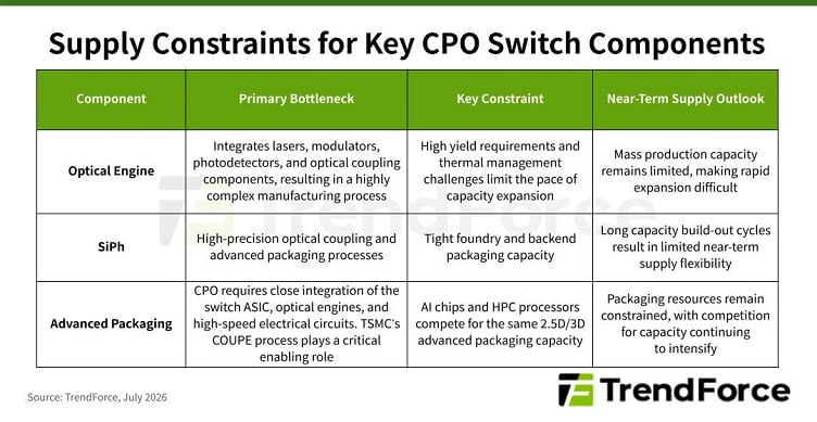
Nvidia and Broadcom have started volume production of co-packaged optics (CPO) switches but supply challenges of key electronic components like optical engines, silicon photonics chips and advanced packaging may impede future production expansion.
This is according to a new report from market research TrendForce that said Nvidia’s Spectrum-X CPO switch, co-developed with Taiwan Semiconductor Manufacturing Company (TSMC) using its COUPE packaging technology, and Broadcom’s Bailly CPO switches are in the mass production phase and are expected to further expand in late 2026.
The Spectrum-X CPO switch delivers up to 400 Tb/s of switching capacity while the Bailly CPO switch compared with conventional pluggable optical transceivers reduces power consumption by up to 70% and already has completed deployment validation with hyperscalers like Meta.
The importance of CPO switches
CPO switches integrate optical engines directly into the same package as the switch application-specific integrated circuit (ASIC) instead of routing signals to pluggable transceivers sitting on the faceplate.
That shorter electrical path allows switch bandwidths to climb past 51.2 Tb/s to 102.4 Tb/s. CPO cuts the distance between the ASIC and pluggable optics, significantly lowering the power per bit, reducing latency and freeing up faceplate space.
Not surprisingly, CPO switches have emerged as the leading architecture for next-generation high-bandwidth switches, TrendForce said. It is also considered one of the few viable paths to keep scaling switch throughput without considerable power concerns.
Major bottlenecks ahead
TrendForce said there are three potential bottlenecks facing CPOs:
- Optical engine
- Silicon photonics
- Advanced packaging
The optical engine integrates lasers, modulators, photodetectors and optical coupling components into one module. This means thermal management as well as high yields are a must and could limit mass production to only a handful of suppliers, TrendForce said.
Silicon photonics, meanwhile, require a high level of precision and reliability. With fabs having long build cycles, it leaves little flexibility to increase supply in the near term, the market research firm said.
Finally, advanced packaging is a bottleneck due to the same packaging used in AI chips and high-performance computing (HPC) processors will be needed for CPO switches. These 2.5/3D packages are likely to be in tight supply in the near term, TrendForce said.
Supply chain ramp up
In terms of silicon photonics, foundries are already planning ahead for the future. TSMC, GlobalFoundries (GF) and United Microelectronics Corp (UMC) have been accelerating support for the technology.
In November 2025, GF acquired Advanced Micro Foundry (AMF) to create what it claims to be the largest pure-play silicon photonics foundry. The AMF acquisition not only expands GF’s silicon photonics portfolio, but also increases its production capacity and R&D in Singapore.
GF said silicon photonics is essential for AI infrastructure and as data continues to move faster and workloads become more complex, moving data at greater speeds, precision and power efficiency will be critical to future data centers and telecom networks.
TSMC, the world’s leading foundry and chipmaker, and Samsung foundry’s division are also creating their own silicon photonics ecosystems but they are on different paths. TSMC is using its customer relationships and leading-edge technologies through CPO via its COUPE platform. Through its close ties to Nvidia, TSMC is likely to bundle photonics into graphics processing units (GPUs) or other modules to close the gap between heat, latency and power draw.
Samsung is playing catch up in some ways with its roadmap to begin mass production of silicon photonics in 2028. Samsung will also bundle with high bandwidth memory (HMB), system semiconductor foundry services and packaging in an all-in-one strategy. Samsung formally entered the silicon photonics market in March 2026 after completing a process design kit. Samsung is also rolling out full CPO services by 2029.
In July 2026, UMC delivered what it claimed was the first mass produced silicon photonic chips on 300 mm wafers at its Singapore fab, combining Silith’s technology with UMC manufacturing.
TrendForce believes vertical integration is becoming the default playbook. Vendors that can control silicon photonics design, optical engine manufacturing and advanced packaging in-house will be best positioned to lead once the CPO switch market hits its volume ramp in 2027 to 2028.
