Quantum technology startup EuQlid has launched a quantum sensing platform designed for 3D imaging of semiconductors and batteries.
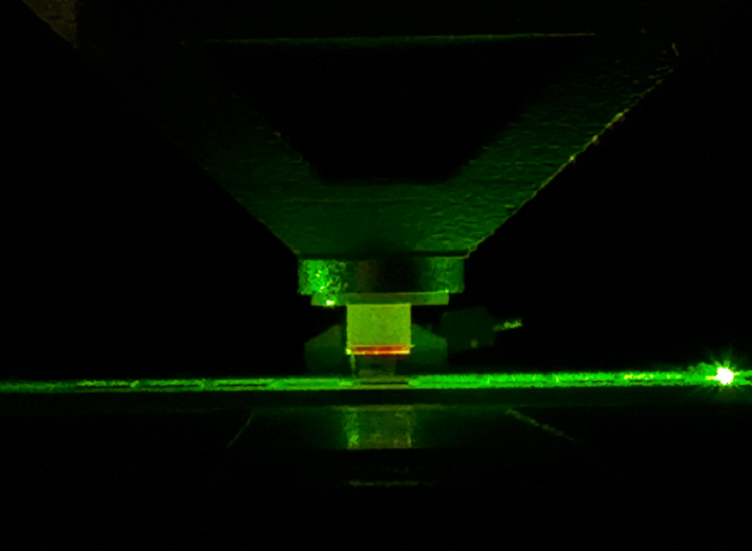
EuQlid, who raised $3 million, has debuted its quantum imaging platform called QU-MRITM that enables non-destructive mapping of buried current flow inside materials and devices.
The company said the technology is needed to address a gap in the semiconductor and energy storage industries that allows for visualizing sub-surface currents with precision and speed that inspection and test tools today cannot reach.
This will also allow for new product development and high-volume manufacturing yields, EuQlid said.
Why is it needed?
EuQlid said the demand from AI is accelerating chip logic, memory and advanced packaging to adopt 3D architectures.
New metrology and inspection tools will be required to control and optimize these new manufacturing workflows. The company points to global demand for metrology and inspection tools exceeding $10 billion annually and is expected to grow substantially with the adoption of 3D architectures.
“We want to make quantum precision available now, addressing fundamental 3D metrology and inspection whitespace, to enable the next era of semiconductor and battery revolution,” said Sanjive Agarwala, co-founder and CEO.
