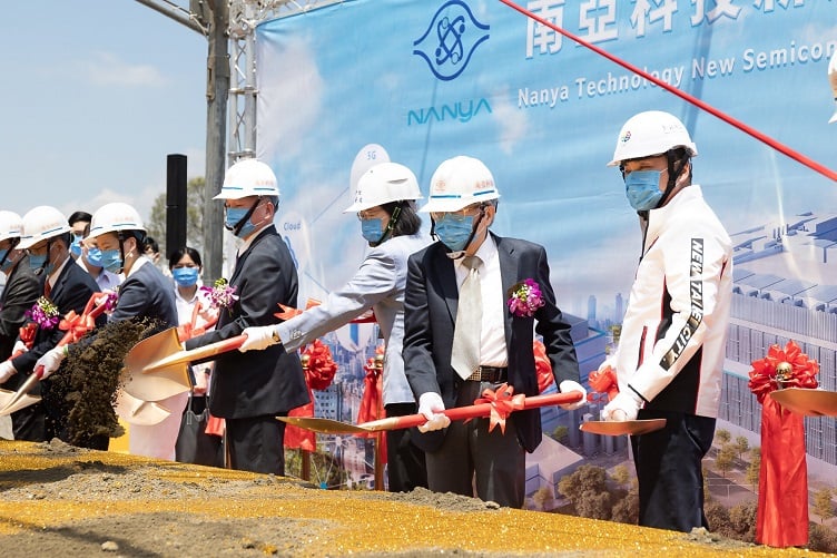
Nanya Technology Corp. has broken ground on its $10.1 billion semiconductor fab in New Taipei City’s Nanlin Technology Park that will be used for DRAM production.
The facility will include a main fab with a double-deck cleanroom, R&D center and water recycling center. A separate building with extreme ultraviolet (EUV) lithography equipment will be established for future advanced process nodes. The fab will allow Nanya to implement several generations of 10 nm-class process technologies and adapt artificial intelligence to improve manufacturing performance.
Upon completion, which is scheduled by 2025, the fab will be capable of producing 45,000 wafers per month with DRAM bit growth achieving 120% and creating about $2.4 billion annual production value. Additionally, the fab will create 3,000 high-tech jobs and support thousands of indirect job opportunities in the New Taipei City region.
Nanya is currently forecasting to be in production of its first generation 10 nm-class technology process by the end of 2022 and has begun trial production on the second-generation of the process node. The third generation and EUV lithography fourth generation are under development. These technology developments will be grafted to the new fab when operational.
Nanya is the fourth ranked DRAM brand by revenue, according to market research from TrendForce. The company had a 3.0% market share behind Samsung, SK Hynix and Micron Technology.
