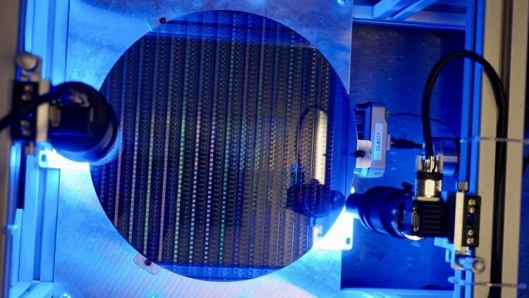
Ongoing semiconductor supply chain issues prompted University of Colorado mechanical engineering students to design a device that improves the wafer inspection process. The silicon wafer center-finding improvement system developed for semiconductor manufacturer KLA enhances the efficiency of wafer inspection for defects.
The prototype uses two cameras to capture the circular wafer’s edge, plus computer software to calculate the radius and find the wafer’s center. The technology currently used by KLA to detect the center relies on obtaining 10 different images around the edge. The student-designed approach accomplishes this task with only two images, and efforts are underway to reduce the eight-second time required to align one wafer down to two seconds. Device accuracy is also under scrutiny with ongoing statistical tests and measurements to ensure that coordinates are within 10 μm of the true center.
A reduction in inspection time is crucial for increasing throughput to cope with the global silicon wafer supply shortage and the steady demand for semiconductor chips.
The student designers presented their silicon wafer center-finding improvement device at the College of Engineering and Applied Science Engineering Projects Expo 2022 on April 22.
