Researchers from the University of Michigan created a self-erasing microchip that could help stop counterfeit electronics and alert users if a package has been tampered with. The team used new material that temporarily emits energy, changes when exposed to light and self erases in days or is instantly erased with a flash of blue light.
The self-erasing chip is made of a three atom-thick layer semiconductor laid on a thin film of azobenzenes. The semiconductor acts like graphene, but it goes one step further because it can emit light at a particular frequency to create a written message.
Azobenzenes are molecules that shrink when exposed to UV light. These molecules tug on the semiconductor and cause it to emit slightly larger wavelengths of light. With the right kind of light, an encrypted message will be exposed.
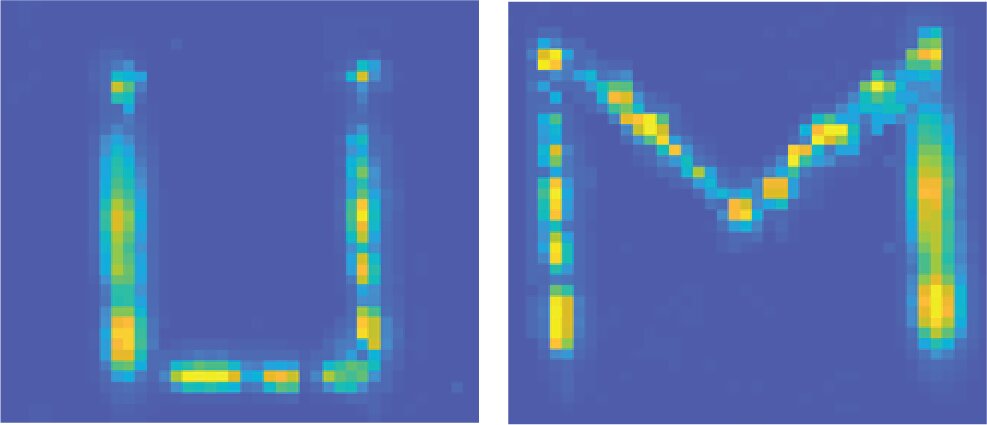 This message will self-destruct in seven days, or it can be erased with a flash of blue light. Written with UV light, the letters are marked out by molecules that shrink by storing energy, stretching the atoms of the semiconductor above. Source: Che-Hsuan Cheng, Excitonics and Photonics Lab, University of Michigan
Stretched azobenzenes give up stored energy over the course of seven days in the dark. This time could be shortened with exposure to heat or light or lengthened by being stored in a cool dark place. The encoded message disappears when azobenzene stops stretching the semiconductor. It can also be erased all at once with a flash of light. Once erased, the chip can record a new message or code.
To create the self-erasing chips, a single layer of molecules was placed in water, and a silicon wafer was dipped in the water and coated with molecules to produce chip layers with semiconductors. The team also used the scotch tape method. Sticky tape was placed on a chunk of semiconductor and used to draw off single layers of the material. The “sandwich” produced was a single layer of tungsten atoms between two layers of selenium atoms. A stamp was used to transfer a semiconductor onto the azobenzene coated chip.
The team said their next step is to extend the amount of time that the material can keep the message intact as an anti-counterfeit measure.
A paper on this research was published in Advanced Optical Materials.
