Sponsored Content
Processors
Nobody Gets Fired for Bringing PCB Prototyping In-House
07 May 2018
Sponsored content
Whether it is creating advanced electronics for automobiles or unmanned aerial vehicles (UAVs), manufacturers in a wide range of industries are turning to the practice of rapid PCB prototyping in their own in-house labs to innovate and speed up a product’s delivery to the market. Their engineering teams are iterating faster and disrupting markets by having the flexibility to design and test circuit concepts and new material ideas with unprecedented freedom. In the process, they are also saving money by cutting outsourcing costs and time, reducing material waste and uncovering invaluable design-for-manufacturability (DFM) challenges earlier on in the research and development (R&D) process.
What follows is a contrasted view of the two different ways to obtain prototype PCBs: through an outside PCB fabrication company, or by investing in an in-house PCB prototyping machine. In short, this brief is aimed at arm engineers and executives with valuable reasoning for catching up with their forward-thinking competitors and industry associates who have already invested in in-house rapid prototyping.
The Nuances of RF/Microwave Prototyping
A prototype PCB is the first tangible representation of a design from an engineer’s imagination, with some help from a computer layout program. It is the opportunity to turn a concept into a reality, and to evaluate that reality through testing to see if it is fully optimized and ready for production. Ideally, a final prototype reflects in large part a final product. Circuit elements, circuit-board material, board layers and the dimensions of the circuit traces and spaces will all be thoroughly defined and vetted by testing the device under application- specific conditions. Once approved, the product moves into the production phase.

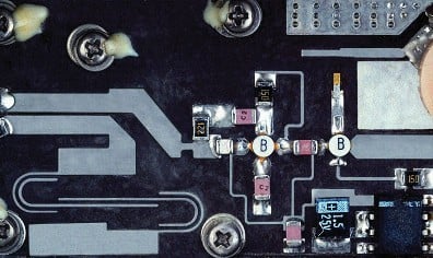 Figure 1. A prototype PCB provides real-world insight into a circuit design, and can be tested to check performance over a wide range of operating conditions.While computer-aided design (CAD) and simulation programs offer automatic rule-checking routines to alert a designer when circuit traces may cross or be placed too close together, when additional grounding is needed or when an IC or circuit component is not properly connected, they can only predict the performance of a prototype circuit and its various component parts so far. Thus, a first circuit or prototype of a design (Figure 1), is built and then characterized with different signals and under different operating temperatures and conditions. Upon receipt, prototype PCBs will undergo testing and the initial design is modified, often several times, before a final first unit is approved for mass- production.
Fabricating a prototype circuit requires a choice of PCB material, a dielectric sheet typically laminated on one or both sides with a conductive metal, such as copper. Circuits are formed by removing the unwanted metal and leaving the desired circuit traces. One of the more popular circuit-board materials is FR-4, a low-cost, epoxy-based substrate that is well suited for a variety of analog and digital applications (Figure 2). Many different types of PCB materials are available but it is important to fabricate a prototype with the same material intended for final production to best track performance as well as cost.
When selecting circuit material for a prototype, two of the more important material parameters to consider are relative dielectric constant (XR) and loss tangent.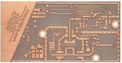 Figure 2. This photograph shows a bare FR-4 board laminated with a conductive metal, such as copper. This is an epoxy- based PCB material used for a wide range of analog and digital circuits (and prototypes). It can be laminated with conductive metal on one or both sides, for creating single- sided or double-sided circuit boards, respectively. The relative dielectric constant, also known as permittivity, indicates the impact that a dielectric circuit material will have on the capacitance of a conductor fabricated on or within the material. Commercial circuit materials can be specified over a wide range of permittivity values. At higher values, an EM wave will travel at slower speeds along a conductive trace, and the trace will exhibit lower impedance and larger stray capacitance than circuit materials with lower permittivity values. For high-frequency analog circuits and high-speed digital circuits, PCB materials with lower values of relative dielectric constant will typically support higher performance levels than materials with higher values of permittivity. To allow designers to benefit from the reduction in circuit dimensions that occurs at higher relative dielectric constants, numerous suppliers of high-frequency circuit materials have developed low-loss materials with high values of relative dielectric constant capable of excellent performance.
Additional material parameters to consider for a prototype PCB material also depend on such factors as the bandwidth or maximum digital speed of the prototype design and its expected power-handling capabilities. For example, variations in PCB material dielectric constant across a panel of the material can result in inconsistent performance from multiple circuits fabricated from that same base-board material. The consistence of the relative dielectric constant with frequency and temperature can also result in variations in the impedance of transmission lines, and variations in the amplitude and phase responses of analog circuits or timing errors in digital circuits. For circuits that must handle higher power levels, such as in a power amplifier, the thermal conductivity of the prototype PCB material is a concern and should be specified for the maximum expected power level of the circuit. In all cases, the PCB material that is used for a prototype should reflect the same choice that would be used for production circuits.
The right choice of substrate material is very important for the overall performance of a circuit, especially for RF/microwave or high-speed digital designs. As material suppliers refine their products for improved perfor- mance or lower cost, it is even possible that a chosen substrate may change over generations of prototypes.
Why is this important to understand? Whether a chosen prototyping process is based on in-house equipment or an outside PCB service, it should provide the flexibility to process all of the possible material choices that an engineer might ultimately wish to experiment with and ultimately employ, to ensure the best chance of prototyping success.
Building Prototypes Outside
Once a prototype circuit design had been committed to a Gerber or other standard layout file, the traditional means of having a prototype PCB built meant choosing a “board shop” or PCB fabricator. With the widespread adoption of internet-based websites and services, the search for a PCB fabricator has become greatly simplified. Most PCB fabricators show full listings of their capabilities on their websites. Some even offer free downloadable layout software to simplify the process of transferring circuit layout files to them. Many even suggest sending Gerber or other layout files to them in advance to help them determine prices for the job.
Those free software programs offered by many PCB shops may appear to have cost benefits, but they also have limitations. Many of these software tools are proprietary to one company, and don’t provide industry- standard Gerber file exports. So a circuit designer working with that software is stuck with that one PCB shop and cannot transfer layout files to other vendors. This can lead to problems and delays, especially if a chosen PCB shop is not able to process all of the substrates that a designer might choose. This is particularly true of circuit substrates for RF/microwave designs, since they often require specialized manufacturing equipment. A solution often requires a completely new design in a different software package that supports industry-standard file exports, such as Gerber or DXF, so that files can be sent to a different vendor.
Working with an outside board shop brings with it the benefits of that shop’s expertise and experience. Based on a customer’s performance requirements for a prototype circuit, that shop may recommend a type of high-frequency circuit board material, or several materials that can meet a customer’s performance requirements, but at different price points. Of course, a customer not familiar with those materials must trust in the expertise of the board shop that those materials will yield the performance expected of a prototype circuit under all operating conditions, including across frequency and temperature. 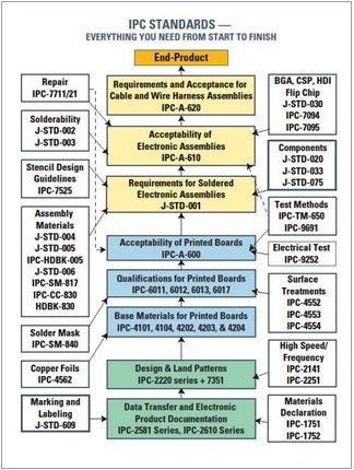 Figure 3. Not all board shops can certify to IPC standards. This guide will help you verify.
Some other considerations when selecting an outside PCB fabricator are facilities’ capabilities in terms of inspection and environmental testing, if needed. For example, does the facility provide an up-to-date, ISO-compliant quality system? Is it UL registered? Can it build PCBs to IPC-A-600 or 6012 standards as required? (Figure 3) Essentially, the quality control that would be exercised over the creation of an in-house prototype PCB is being trusted to an outside facility, and some of these qualifications can provide some assurance of a facility’s capabilities to meet high standards. ITAR registration is another important consideration when choosing an outside PCB vendor that will be handling government sensitive circuits. Many PCB prototype vendors offer services through websites, where the actual manufacturing of the prototype often will be performed overseas, even when the storefront of the board house is located domestically.
Many PCB fabricators offer special 24-hour turnaround times for time-sensitive prototypes, but these fast turnaround conditions, when available, are also much more costly than standard turnaround times of one to two weeks. Some PCB fabricators will also differentiate between prototype PCBs fabricated in the United States versus those built overseas, with lower prices quoted to customers willing to accept the much longer turnaround times associated with overseas PCB fabrication.
Although each PCB prototype fabrication quote has a relatively low cost associated with it, many PCB fabricators require a minimum order of 10 to 20 circuit boards so that, even for a prototype that has yet to be tested for performance, duplicate boards must be produced when perhaps only one or two are needed to verify the performance of the prototype PCB. The general problems associated with outside PCB fabricators are not with the quality of the fabrication, but in the often long and unpredictable lead times to receive a circuit board after a layout file has been transmitted and other requirements have been agreed upon.
Most design engineers will admit that it is rare when only one iteration of a prototype is needed as part of a product development cycle. More typically, when a prototype is first built, it goes through a series of modification cycles to correct design or fabrication mistakes. For this reason, the delay times from an outside PCB fabricator can be costly more in terms of product development than in the cost of the fabricator’s fees. Those delays can translate into delays in product development and in time to market, which can be extremely costly in competitive areas of electronic sales. In addition, delays between prototype engineering versions can make it difficult to compile and keep track of engineering modifications and can result in overlooked production problems.
Prototyping In-House
A growing number of electronics manufacturing companies, ranging from analog audio to high-speed digital and high-frequency RF/microwave circuit manufacturers, have come to appreciate the benefits of bringing prototype circuit fabrication capabilities in-house in place of using an outside PCB fabricator. One of the most obvious benefits is the tremendous increase in turnaround time, in some cases from days or weeks at an outside PCB fabricator, to as little as hours or even minutes with an in-house circuit-milling machine or laser system. Of course, having the in-house capability versus placing an order with an outside firm also expands the range of possibilities of which circuits can be fabricated as prototypes, so that possible alternative designs can be fabricated as prototypes to experiment with different weights of copper on a dielectric board or other changes in key design parameters that might be too expensive to try at an outside PCB fabricator.
In-house prototyping helps save time when a design requires multiple prototype generations. Many first prototypes uncover shortcomings in a design, triggering a second-generation prototype. These shortcomings may be electrical or mechanical in nature, such as those from unexpected coupling or radiation effects.
Addressing different design problems can lead to two, three, or even more design iterations. Saving time on each prototype generation can amount to a significant reduction in the overall design cycle, making a strong case for the use of in-house PCB prototyping equipment.
Spotlight: Knowing a Shure Thing When They Saw It
Having the in-house capability to produce PCBs can also bring hidden benefits, as Robert Kobak, senior technician at Shure Inc., a world leader in professional audio electronics, explains:
“One of the more valuable things about having the machine at our fingertips is we’ve learned to use it to fix finished boards, too. We had a run of 100 boards come in missing a critical mounting hole, for example, and we were able to drill them easily with the LPKF machine and get them out the door.”
In one extreme case, Kobak was able to fix a multilayer circuit design that was missing via holes.
“Some people thought it couldn’t be done,” said Kobak. “But I reworked the Gerber files to reposition the via holes on an open spot and was able to save the design. It would have been infeasible to go back to the board shop.”
Of course, the largest single hurdle to switching from using an outside prototype PCB supplier to an in-house machine is the cost of the mechanical milling or laser etching machine and proving the potential payback to management.
Kobak points out that the initial hesitation of investing in an in-house circuit-milling system was quickly overcome. They ordered one LPKF milling machine, and then quickly ordered a second machine when they saw how well the first one worked.
“We were going outside for prototype PCBs, which got expensive. Our outside board shop was often charging us for a minimum number of boards, whether we needed that many or not. One project, a four-layer, minimum 150-board run was near $10,000, while the cost of our first LPKF machine was under $30,000, including accessories and consumables!”
For some design teams, having an in-house circuit-board milling machine not only represents increased speed and flexibility in creating prototype circuits, it is also a means of building circuits that help evaluate new components for those circuits. Most companies try to know as much as they can about a new component from an outside supplier, be it a discrete transistor or an IC, before committing that component to a PCB design. Having an in-house circuit-board milling machine makes it possible to create small runs of evaluation circuits — and evaluate how components perform under realistic working conditions. These subtle but important tweaks are often left undone in the interest of time when you outsource.
Spotlight: Just Ask Raytheon
Garry Ingram, technical support engineer for Raytheon Indiana, said that his company has used an LPKF PCB machine for almost two decades both for its initial intended purpose of fabricating prototype circuit boards, and as part of the process of evaluating new RF and microwave components and materials.
“With any new components, you must see how they’ll perform in the environment in which they will be used, including the PCB dielectric material on which they will be mounted. The LPKF equipment allows us to make evaluation boards for these experiments very fast,” according to Ingram.
How to Shop for a PCB Prototyping Machine and Ensure it Has the Capabilities You Need
Commercial circuit-milling machines are available as mechanical or laser-based systems, typically with high-performance stepper motors used to achieve precise positioning on a circuit board. Both types of PCB fabrication machines are designed to work with copper-coated circuit-board materials. They form circuits by means of milling, a subtractive process that removes unneeded copper from the board, rather than the chemical-etching processes of many outside PCB fabricators and in-house “wet-etch” departments. A number of parameters can be used to compare different circuit-milling machines, such as the dimensions of the largest board it can process, the circuit feature resolution it can achieve and the milling speed, among others. These parameters will be determined by a company’s anticipated requirements of present and future prototype PCBs. A system capable of handling a large circuit board size, for example, can fabricate a large number of different circuits or a number of versions of one circuit at the same time. A circuit-milling machine’s spindle speed will determine how many holes can be drilled in a given time, such as 100 holes per minute, and how fine a trace can be milled reliably. Comparing the parameters of different circuit-milling systems will provide insight into the quality and quantity of prototype circuits that each system can produce in a certain time.
For example, circuit feature resolution of 2 μm or better will usually exceed the capabilities of most outside PCB fabricators. It will also typically exceed the fabrication needs of most prototype and experimental circuits.
Repeatability of ±2 μm will ensure that circuit features remain consistent from circuit to circuit and board to board. These dimensional tolerances can support high-speed digital circuits at speeds beyond 40 Gb/s and analog microwave circuits at frequencies well into the millimeter-wave range, beyond 40 GHz. Such tolerances may exceed current needs, but provide room for future growth and experimentation.
 Figure 4. A mechanical milling PCB machine.Any circuit-milling machine under consideration for in-house PCB prototyping (Figures 4 and 5) should handle a wide range of dielectric materials, from low-cost FR-4 materials through low-loss polytetrafluoroethylene soft boards and harder ceramic-filled circuit materials. It should be able to read standard CAD and computer-aided manufacturing (CAM) files from industry-standard software suppliers (or at least the set of software tools being used by the company considering the circuit-milling machine) as well as standard layout file formats, including Gerber, HP- GL and DXF files.
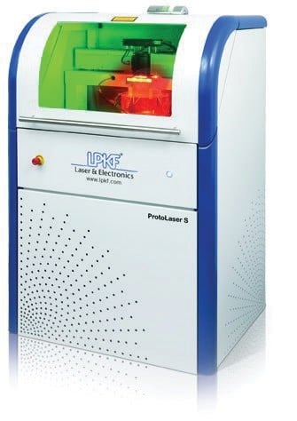 Figure 5. This laser prototyping system offers improved precision and speed when creating prototypes.As with any piece of capital equipment, an in-house circuit-milling machine carries with it a learning curve but, if supported with suitable operating software, the training time can be minimized. The LPKF circuit-milling machines, for example, are supplied with CircuitPro, a multifunction software package that provides intuitive control and time-saving utility programs that enhance the efficiency of each system (Figure 6). The software allows operators to import data from any circuit-layout program. The LPKF software tools load and run on any standard Microsoft Windows®-based PC and provides control of each milling machine with clear, on-screen instructions. The software also includes a “what-you-see-is-what-you-get” interface to show the manufacturing progress and manage all relevant parameters of the machine and its tools (Figure 7). The software orchestrates a variety of functions, including automatic tool changes, automatic tool calibrations and management of tool life as well as feed rate and tool RPM.
In Summary
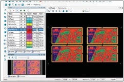 Figure 6. CircuitPro software imports and edits a wide range of circuit layout file formats for use in LPKF’s manual and laser-based PCB milling systems. Depending upon the milling machine, the software supports fabrication of circuit features with better than 1 μm resolution.In-house rapid prototyping capability brings with it fast turnaround speed, the flexibility to try different design variations, and even the capability to fix circuit designs considered “unfixable.” In many cases, in-house circuit milling machines can top the precision and resolution of outside board shops, and do it faster.
Surveys of LPKF customers have revealed the impact of in-house savings by as much as two weeks for creating a prototype in house, compared to an outside facility (Figure 8). Better than 41 percent of surveyed customers reported a time savings of four to seven days on prototyping projects compared to using an outside board shop, while almost 23 percent attributed a savings of one to two weeks when using the LPKF systems compared to an outside shop. And nearly 23 percent of surveyed customers credited the LPKF machines for a time savings of two weeks or more in their prototyping efforts, compared to using an outside service.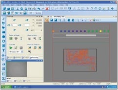 Figure 7. LPKF’s software simplifies the use of the PCB milling systems through a straightforward operating interface.
In addition to improved time to market, the LPKF customer surveys indicate that in-house PCB milling machines can bring a healthy increase in design productivity and creativity as engineers see tangible results of their designs in real-time.
More than 70 percent of LPKF customers credited their rapid prototyping machines with fostering a more innovative design culture in their companies, while better than 57 percent of those customers linked the machines to increased productivity and another 59 percent with greater project momentum.
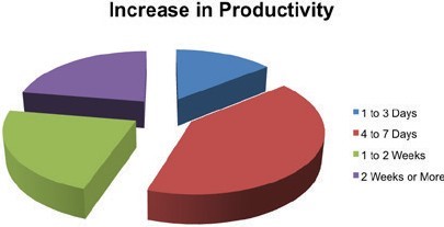 Figure 8. When surveyed, more than half of LPKF customers saved one week or more for their prototyping tasks compared to using an outside board shop.Yes, PCB milling machine represents an investment, but it’s one that can bring healthy return on investment in the near term and for many years to come.
Next Steps
- Visit PCB PrototypingMachines.com and use the PCB System Selector to find the machine that’s right for you and request pricing.
- Review the LPKF CapEx Justification Kit and get started on your Business Case for a new machine.
- Download the Tech Brief “PCB Substrates: Matching your design to the right material and rapid prototyping process.”
Powered by CR4, the Engineering Community
Discussion – 0 comments
By posting a comment you confirm that you have read and accept our Posting Rules and Terms of Use.
Advertisement
Advertisement
Popular News
Find Free Electronics Datasheets

Advertisement