Adding a step to the inkjet printing process enables printing of lines with a specific height and with much smoother features than would otherwise be possible. The modified method developed at CSEM Muttenz, Switzerland, can be used to print waveguides and other optical components. It can also be applied to the fabrication of electronics and microfluidics, and to advance devices such as optical sensors used for health 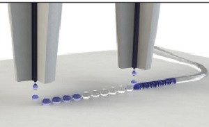 Subsequent droplet deposition leads to self-aligned capillary bridges and allows the assembling of complex structures. Source: CSEMmonitoring and lab-on-a-chip tools that integrate and automate multiple laboratory functions onto a small circuit.
The researchers deposited ink in two steps, rather than the traditional single step, resulting in structures considered to have 2.5 dimensions because although they are not flat, their complexity is limited compared to structures created with traditional 3D printing. Inks deposited on a substrate tend to bulge or split because of surface tension. The two-step technique takes advantage of surface tension: ink printed in the second step seeks to minimize its surface energy by self-aligning between the droplets from the first print. Pre-patterning of the substrate is not required, which increases the available design space and simplifies fabrication.
The researchers fabricated a polymer waveguide that was 120 microns wide and 31 microns tall with a taper that allowed light from an external laser source to enter the waveguide. Optical loss within the waveguide was measured at 0.19 dB/cm, only an order of magnitude higher than state of the art waveguides created using photolithography.
The printing process can also be used with other materials such as metallic inks to make electronics or sucrose mixtures for biodegradable applications.The researchers are now working to optimize the printing method and the ink to further lower the amount of light lost by the waveguide.
The research is published in Optics Express.
