6G holds many promises for self-driving cars, instant healthcare diagnosis, super-fast download speeds and more current and emerging applications. But to get there requires developing powerful semiconductors.
Researchers at the University of Bristol are developing a new type of semiconductor architecture that uses special gallium nitride (GaN) amplifiers. The technology was achieved by discovering a latch-effect in GaN to unlock greater radio frequency (RF) device performance.
These devices use parallel channels that require the use of sub-100 nm side fins, a type of transistor that controls the flow of current passing through the devices.
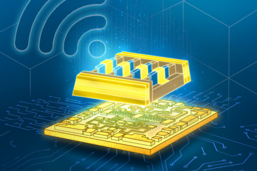 An artistic image of a futuristic semiconductor device which will help make 6G technology a reality. Source: University of Bristol“Within the next decade, previously almost unimaginable technologies to transform a wide range of human experiences could be widely available,” said Martin Kuball, professor of physics at the University of Bristol. “The possible benefits are also far-reaching, including advances in healthcare with remote diagnostics and surgery, virtual classrooms and even virtual holiday tourism.”
Kuball added that potential road safety improvements from advanced driver assistance systems (ADAS) and industrial automation are possible with 6G.
1,000 fins
The architecture, called superlattice castellated field effect transistors (SLCFETs), has more than 1,000 fins with sub-100 nm width help drive the current, enabling a high RF performance. However, the physics behind this high performance was unknown but equated to the latch-effect in GaN.
Researchers will seek to pinpoint where the effect occurred using precision electrical measurements and optical microscopy.
“We also developed a 3D model using a simulator to further verify our observations,” Kuball said. “The next challenge was to study the reliability aspects of latch effect for practical applications. The rigorous testing of the device over a long duration of time showed it has no detrimental effect on device reliability or performance.”
He added that the key aspect driving reliability was a thin layer of dielectric coating around each of the fins. This latch effect could be exploited for practical applications for years to come, Kuball said.
The next steps
The University of Bristol plans to further increase the power density the semiconductors can deliver to achieve a higher performance and serve a wider audience. It will also work with industry partners to bring next generation devices to the commercial market.
The full research can be found in the journal Nature Electronics.
