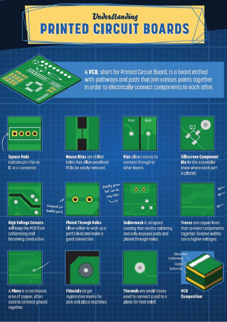
A printed circuit board (PCB) is used to mechanically support and electrically connect electronic components using conductive pathways, tracks or signal traces etched from copper sheets laminated onto a non-conductive substrate.
Each PCB contains electrical circuitry made up of embedded metal wires called traces, and larger areas of metal called planes. Electronic components are soldered to the top, bottom or both layers of the board onto metal pads. These pads are connected to the board circuitry allowing the components to be interconnected together. The board may be composed of a single layer of circuitry, circuitry on the top and bottom, or of multiple layers of circuitry stacked together.
Circuit boards are built with a dielectric core material with poor electrical conducting properties to make the circuitry transmission as pure as possible, and then interspaced with additional layers of metal and dielectric as needed. The standard dielectric material used for circuit boards is a flame-resistant composite of woven fiberglass cloth and epoxy resin known as FR-4, while the metal traces and planes for the circuitry are usually composed of copper.
Discover more about PCB technology and manufacturers on GlobalSpec.com.
