
Some technologies have been around for such a long time, it is a monstrous task to try and replace them altogether. It is not likely that the silicon electronics currently in use will be replaced, but it is possible to ensure that future electronics can use a more sustainable and environmentally friendly option moving forward. Slowly, we can fight the rise in electronics and the waste that is produced from creating and disposing of them. The problem is, less than 25% of all electronics thrown away each year are recycled, and this issue is only getting worse due to new 5G devices coming to market and the internet of things (IoT) continuing to expand at a fast pace.
Silicon-based electronics have been a reality for quite some time, and the idea of being able to print electronics onto paper was a dream, until recently. A team of engineers have come up with a specific mixture of carbon-based inks that give them the ability to print electronic circuits onto paper, thus making these circuits also fully recyclable. These devices are said to be high-performance, robust devices that can last for several months, and they decompose when they are no longer needed. During this decomposition, the carbon material is collected from the paper in order to be used for future printing.
Even though this may seem like an advancement in technology that will render silicon electronics irrelevant, that is not what these devices are intended for. They are a new means of satisfying the demand for embedded electronics that are ubiquitous, without manufacturing such a large number of devices that contain toxic waste.
Will this revolutionize the semiconductor industry?
While exciting, this innovation will not be shaking up the half a trillion dollar semiconductor industry. As the world progresses and advances, more data is being consumed and sensors have to keep up with this demand. That means that more devices must be created, and paper electronics are aimed at reducing the impact that this has on the environment moving forward. If one thing is for sure, innovation in technology is not slowing down any time soon, nor should we want it to.
It was realized in recent years that in order to minimize the impact of this rising demand, more research on transient and printed electronics must be undertaken. Low-cost, eco-friendly sensors were a top priority as transient electronics are designed specifically to disintegrate and decompose instead of staying in the environment or in someone’s body. However, they do still produce some waste including silicon. Attempts to create paper electronics previously used some methods that were outside of just using a printer, which was not as efficient as the recent team of engineers would like. They wanted to design a “print-in-place” system that consisted of the substrate being printed out of the printer, and once printing is finished, the device is ready for testing. They were able to achieve this and produce transistors that had the same if not higher performance than other printed examples.
How are these devices made?
Carbon inks from each of the three main parts of thin-film transistors were used to create conductors, insulators and semiconductors. The conductive and semiconductive inks were created from off the shelf materials like graphene and carbon nanotubes. What gives these new devices the edge over their competition and predecessors is the new insulator ink.
Nanocellulose was used for the insulator, which is a biodegradable, plentiful material that is created from wood pulp. It is typically found in cosmetics, wood products, food packaging and within electronics. However, this team was the first to suspend the nanocellulose in a solution and then use it as the ink for their circuit printing.
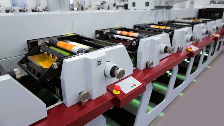
The machine that is used for this process can only be described as an advanced version of a typical inkjet printer that is found in most offices. It is able to deposit the three layers of ink, one layer at a time, onto the paper in order to create the new transistors. The ink is vaporized by the machine into a light mist consisting of tiny droplets and pushes this aerosol toward the surface of the paper using an inert gas. Although this is not the most efficient way to accomplish this, if the basic principle of this machine was transferred to a quicker roll-to-roll printing system, similar to what is used to print on fabric/clothing, thousands of devices could be created in a short amount of time.
 If this technology can be transferred to roll-to-roll printing, these devices can be made extremely quickly. Source: Adobe Stock
Even the team of engineers themselves stated that the durability of these devices shocked them, explaining that the shelf-life of the bare transistors without protective coating or shielding was up to nine months without any measurable loss in performance.
How is the carbon recovered?
In order to separate all of the different components in the devices, they are submerged in a series of baths, and sound waves are used to create vibrations to literally shake them apart. The graphene and carbon nanotubes are filtered out and collected for future re-use. The paper substrate and nanocellulose can then be recycled as materials of their nature typically are.
Applications for this technology are almost endless as sensors are being integrated into every field, and with more testing and development, these devices will become even more efficient and powerful.
What is a stand-out application that you think these paper-printed, recyclable electronics would be perfect for? What advantages will they provide over their silicon-based counterparts? Engineering360 would love to hear your opinions and thoughts in the comments below!
