 The facility will use seismic isolation structure to help with earthquakes and reduce environmental loads. Source: Toshiba
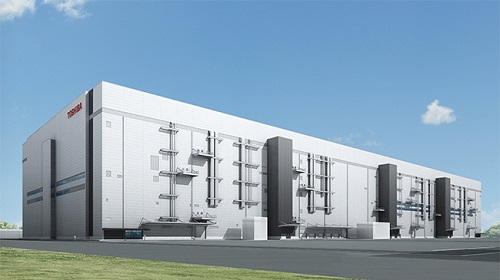
Toshiba Memory Corp. has broken ground on its first semiconductor fab in Kitakami Iwate, Japan, dedicated to the production of 3D flash memory.
The facility, called K1, is slated for completion in the fall of 2019.
Toshiba said the demand for 3D flash memory is increasing in enterprise servers, datacenters and smartphones. The new facility will allow the Japanese company to continue to supply the market in the mid and long term.
K1 is expected to be the largest memory fab as well as the most advanced. The facility will be constructed with a seismic isolation structure that will absorb earthquake tremors and reduce environmental loads by deploying energy-saving manufacturing. The fab will use artificial intelligence to boost productivity, Toshiba said.
Toshiba will continue to look for investments that will help with its capital expenditure spending and R&D line including an ongoing relationship with Western Digital Corp.
