A team of researchers in the Oxide Nano Electronics Laboratory at the University of California, San Diego, have developed a novel approach to fabricate oxide Josephson junctions, which are the basic building block of superconducting electronics.
The team irradiated and disordered a nanoscale region of a superconductor in order to develop a quantum mechanical tunnel barrier. They then were able to write Josephson circuits directly into a thin oxide superconductor.
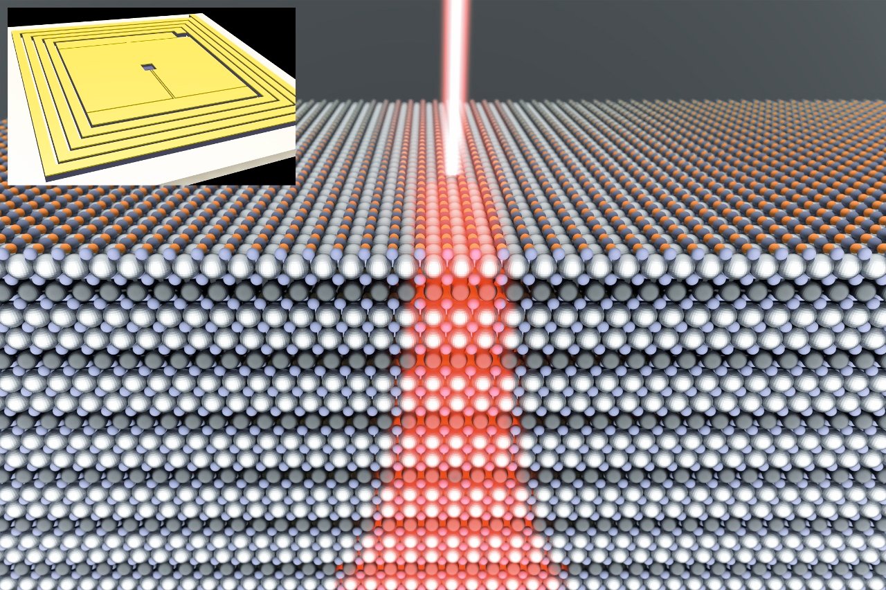 Researchers have developed a novel approach to fabricate oxide Josephson junctions, which are the basic building block of superconducting electronics. Credit: Meng Ma, UC San Diego."By using this direct-write method, we were able to eliminate lithographic processing and now offer the promise of a pathway to quantum mechanical circuits operating at more practical temperatures," says Shane Cybart, principal investigator working within the Department of Physics at the university.
Cybart says that a Josephson junction is composed of "two superconducting electrodes separated by a very small distance—about a billionth of a meter.” The key to the group's direct-write method is that oxide superconductors are sensitive to point defects in the crystal lattice caused by ion irradiation.
"Increasing irradiation levels increases resistivity, while reducing the superconducting transition temperature," says Cybart. "At very high irradiation levels, the superconductor becomes insulating and no longer conducts or superconducts, which allows us to use the small helium beam to directly write junctions into the material."
The diameter of the beam is comparable to the atomic spacing in the material.
This new technique allows for making hundreds of devices a day. The team expects costs to fall, enabling many applications previously considered too expensive.
The team says that this technology will have potential use in biomedical magnetic imaging equipment to non-invasively measure the tiny magnetic fields associated with neural activity in the brain, also known as magnetoencephalography. It also eventually may find use for wide-bandwidth communications and high-performance computing.
